Solar cell and manufacturing method

A solar cell and manufacturing method technology, applied in the direction of final product manufacturing, sustainable manufacturing/processing, semiconductor/solid-state device manufacturing, etc., can solve the problem of easy formation of mirror film layer, inability to directly form suede film layer, increase process complexity, etc. problems, to achieve the effect of reducing production equipment investment, low production cost and high production efficiency

Active Publication Date: 2008-02-06
李毅
View PDF2 Cites 28 Cited by
  • Summary
  • Abstract
  • Description
  • Claims
  • Application Information

AI Technical Summary

Problems solved by technology

[0021] At present, the vacuum coating method or spraying method is usually used to prepare transparent conductive films. Although these methods can produce very uniform film layers, because vacuum film formation is a film formed by the movement of many material atoms to the substrate in a vacuum environment layer, it is easy to form a mirror film layer, and it is impossible to directly form a suede film layer, and additional processing such as subsequent wet chemical etching or laser scribing is required, which increases the complexity of the process

Method used


Image

  • Solar cell and manufacturing method
  • Solar cell and manufacturing method
  • Solar cell and manufacturing method

Examples


example 1

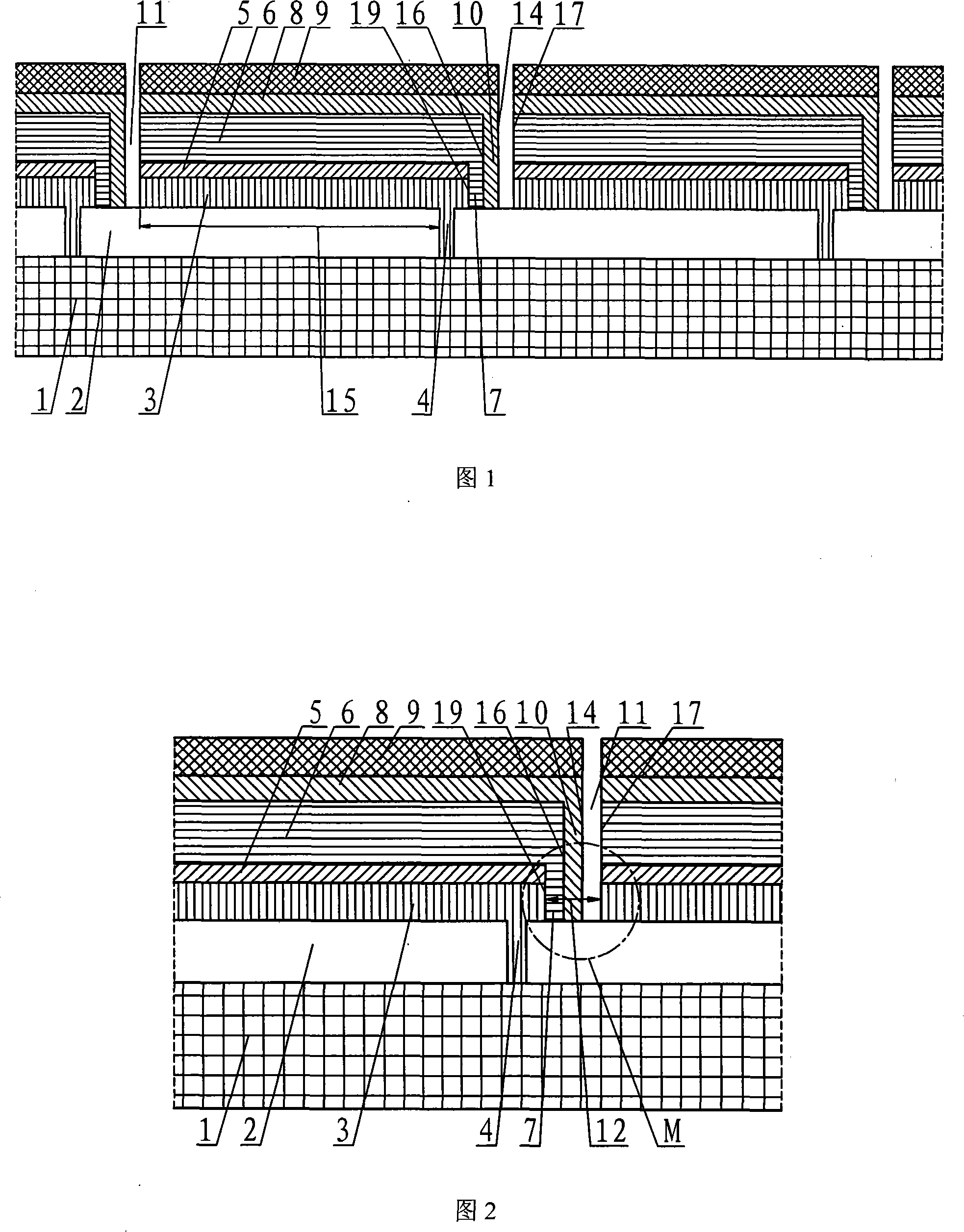
[0061] 1. Scribe the transparent conductive film 2 with a laser scribing method with a size of 14″×48″ or larger in accordance with the electrical performance requirements of the battery panel, with a scribing interval of 20 mm.

[0062] 2. Using plasma chemical vapor deposition (PECVD) at deposition pressures of 70Pa (P layer), 50Pa (I layer) and 80Pa (N layer) at a substrate temperature of 220°C, on the scribed transparent conductive glass in sequence Deposit the P, I, N layers of amorphous silicon of the top cell 3 with a thickness of 80 Ȧ, 700 Ȧ and 200 Ȧ respectively.

[0063] 3. Apply a layer of ITO transparent conductive paste layer 5 with a thickness of 1100 Ȧ on the deposited top cell P, I, N layers of amorphous silicon film 3 by using a high-precision roller rubber machine.

[0064] 4. At a temperature of 150° C., the glass plate coated with the ITO transparent conductive paste 5 is preliminarily cured and baked for 40 minutes.

[0065] 5. Scribe the isolation trenc...

example 2

[0072] Only change the thickness of the ITO transparent conductive paste in step 3 and step 8 in example 1, and the rest of the steps are the same as in example 1:

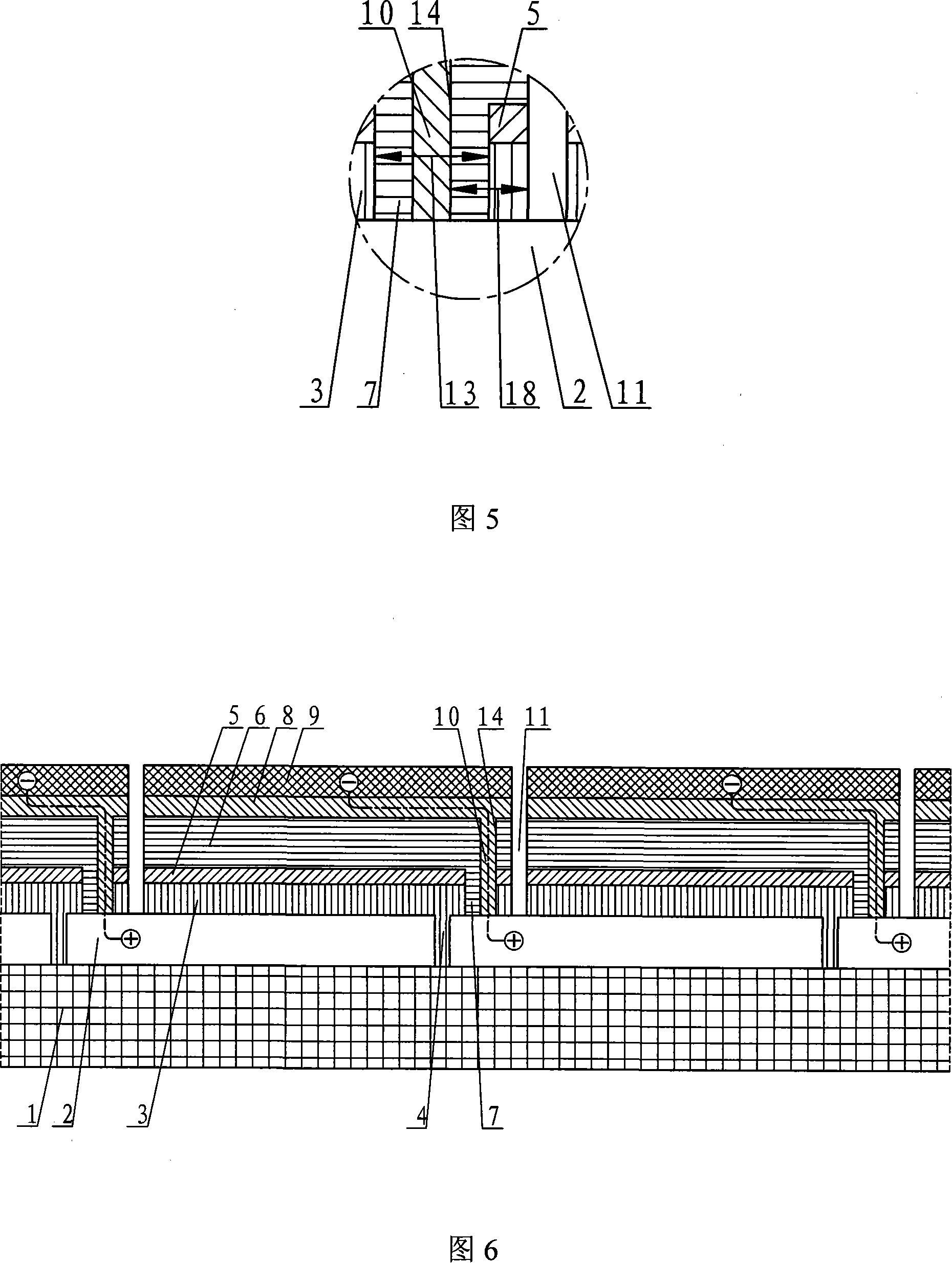
[0073] 3. A layer of ITO transparent conductive layer 5 with a slurry thickness of 900 Ȧ is coated on the N film surface of the deposited top battery 3 by using a high-precision roller glue machine.

[0074] 8. Roll-coat a second layer of ITO transparent conductive film 8 with a thickness of 1000 Ȧ on the film surface of the N layer of the bottom battery 6 that has been laser-marked, and cure and bake at 150° C. for 40 minutes.

example 3

[0076] Only change the width of the laser scribe line in step 5 and step 7 of example 1, and the rest of the steps are the same as example 1.

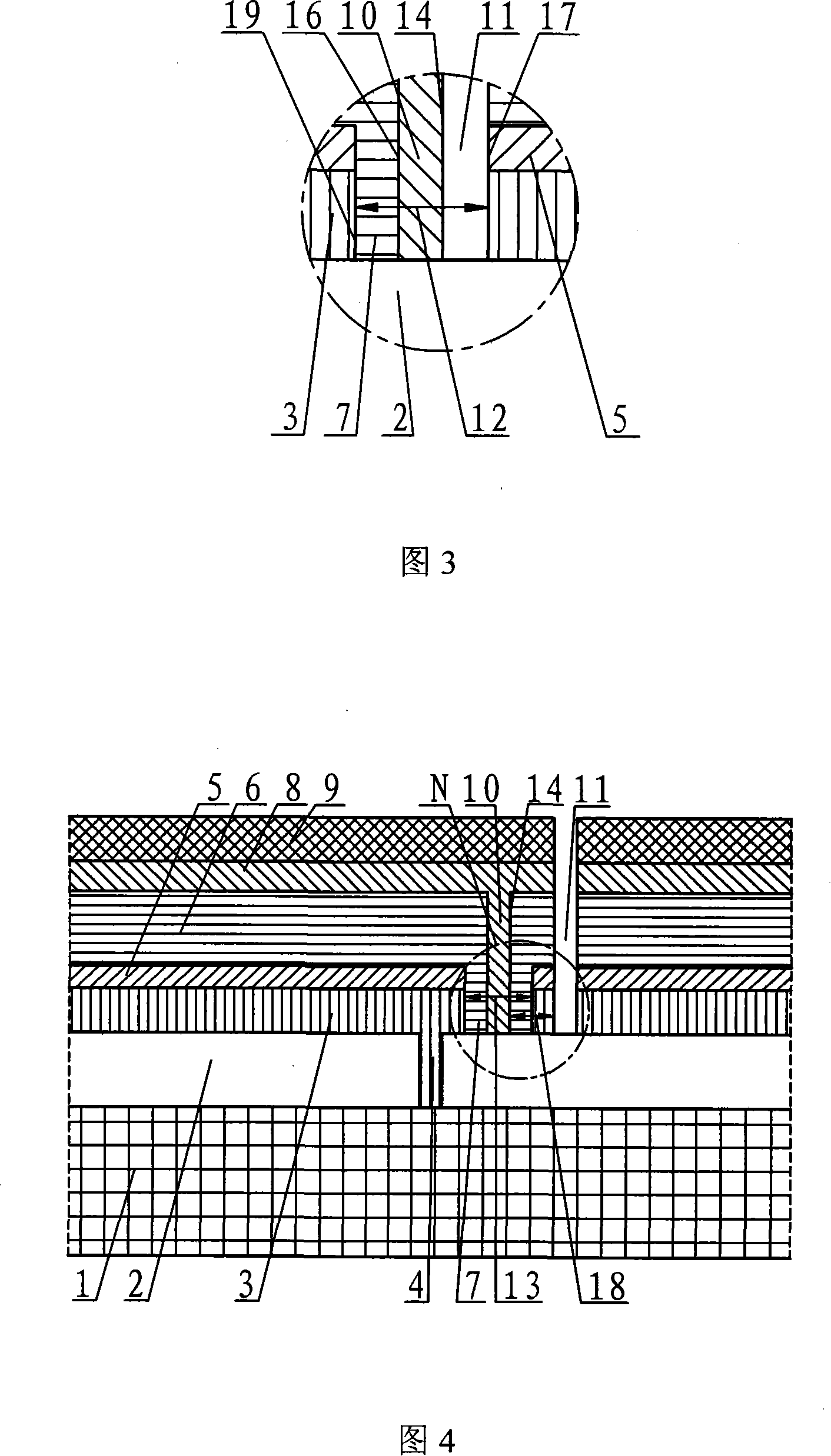
[0077] 5. The laser scriber scribes the isolation trench 7 for insulation, and the laser penetrates the amorphous silicon film layer of the top cell 3 and the transparent conductive reflection layer 5 to perform continuous laser scribing to form the isolation trench 7 with a width of 0.4 mm.

[0078] 7. The laser scriber marks the groove 10 for the electrode connection line, and the glass plate that has already made the P, I, N layers of non-silicon film 6 of the bottom battery is isolated along the laser formed in step 5 with a laser machine. The corresponding position of the channel 7 is used to perform laser scribing on the film layers of the top and bottom cells, and the laser penetrates the P, I, and N layers of amorphous silicon films of the top cell, the middle transparent conductive layer, and the P, I, and N layers of the botto...


PUM

PropertyMeasurementUnit
thicknessaaaaaaaaaa
thicknessaaaaaaaaaa
thicknessaaaaaaaaaa

Abstract

The present invention relates to a multi-stack amorphous silicon solar battery, which adds a transparent reflection film between the stacks and belongs to the thin film solar battery making field. The present inventionhas the technical characteristics that the transparent conductive film between two stacked photoelectric conversion layers is coated on the N face of one amorphous silicon P-I-N photoelectric conversion layer, while the middle transparent conductive film is made of nanometer conductive material. Moreover, a photoelectric unit consists of a stacked amorphous silicon solar battery, and the P film of the amorphous silicon P-I-N photoelectric conversion layer forms a top battery on the back of the front electrode in a roll coating manner. The present inventionis applicable to the mass production, reducing the cost.

Description

technical field [0001] The invention relates to a multi-junction lamination amorphous silicon solar cell, in which a transparent reflective film is added between the laminations and realized by a roller coating method, mass-produced and cost-reduced. It belongs to the field of thin film solar cell manufacturing. Background technique [0002] Thin-film solar cells are one of the mainstream ways to reduce the cost of photovoltaic power generation in the international solar photovoltaic industry today. Due to the shortage and high price of raw materials for crystalline silicon solar cells, the cost of power generation remains high, which has become a fatal bottleneck in its competition with conventional electricity. Thin-film solar cells, especially amorphous silicon thin-film solar cells, are much lower in production cost than crystalline silicon solar cells because their thickness is only about 0.5 μm, the amount of materials used is very small, the manufacturing process is s...

Claims


Application Information

Patent Timeline
Patent Type & Authority Applications(China)
IPC IPC(8): H01L27/142H01L21/82H01L31/0687
CPCY02E10/50Y02E10/544Y02P70/50
Inventor 李毅胡盛明
Owner 李毅
Why Eureka
Try Eureka