Manufacturing method of micro-LED device array unit

A technology of LED devices and array units, which is applied in the production field of micro-LED device array units, and can solve problems such as difficulties, precise grasping, displacement, difficult placement, complex manufacturing process of OLED display screens, etc.

Inactive Publication Date: 2017-09-08
INST OF SEMICONDUCTORS - CHINESE ACAD OF SCI
View PDF6 Cites 22 Cited by
  • Summary
  • Abstract
  • Description
  • Claims
  • Application Information

AI Technical Summary

Problems solved by technology

However, the current high-resolution micro-LED display manufacturing process is much more complicated and difficult than OLED displays
A display often requires millions or even tens of millions of micro-LED chips to be arranged and assembled, especially the precise grasping, shifting, and placement of LEDs with a size of only microns is difficult, resulting in high production costs
This is the main obstacle encountered in the realization of product applications of micro-LED displays

Method used


Image

  • Manufacturing method of micro-LED device array unit
  • Manufacturing method of micro-LED device array unit
  • Manufacturing method of micro-LED device array unit

Examples


Embodiment

[0064] The GaN-based LED epitaxial wafer includes a blue light band and / or a green light band, the wavelength range of the blue light band is 430nm-490nm, and the wavelength range of the green light band is 520nm-580nm. This embodiment is a GaN-based blue LED epitaxial wafer.

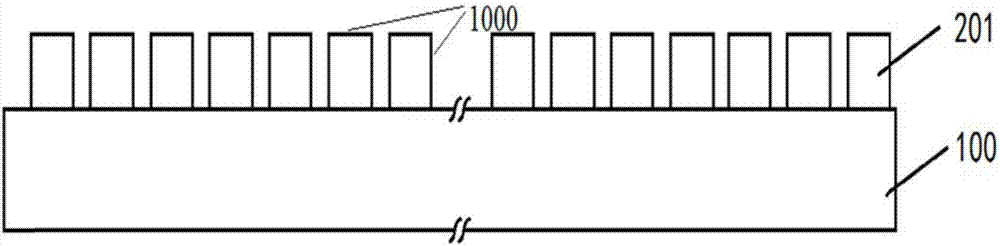
[0065] Select a sapphire substrate 100; deposit various material layers on the sapphire substrate to form a GaN-based blue LED epitaxial wafer; photolithographically etch the GaN-based blue LED epitaxial wafer to the sapphire substrate to form a GaN-based blue light micro LED mesa array 1000, GaN The blue-based micro-LED mesa array 1000 includes a plurality of GaN-based blue-light micro-LED mesas 201 . The arrangement period of the GaN-based blue light micro LED mesa array 1000 is 20 μm×20 μm in the longitudinal direction and the transverse direction respectively.

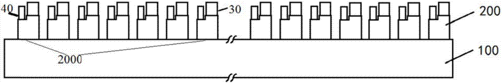
[0066] On each of the above-mentioned GaN-based blue light micro LED mesa array 201, a NiAg metal pn electrode layer and 5 pairs of TiW is...


PUM


Abstract

The invention discloses a manufacturing method of a micro-LED device array unit and a method for manufacturing a display screen by employing the micro-LED device array unit. The manufacturing method of the micro-LED device array unit includes: manufacturing a micro-LED table array; respectively manufacturing a p electrode and an n electrode on each micro-LED table, covering the p electrodes and the n electrodes by a barrier layer and a metal layer, and forming a micro-LED device array; and cutting the micro-LED device array, and forming a plurality of micro-LED device array units. According to the micro-LED device array unit, accurate and mechanical operation difficulties of grabbing, moving and placing of the micro-LEDs due to over-small size thereof can be solved.

Description

technical field [0001] The invention belongs to the technical field of semiconductor optoelectronics, in particular to a method for manufacturing a micro LED device array unit. Background technique [0002] Compared with traditional passive light-emitting liquid crystal display technology, active light-emitting display technology has higher energy efficiency, higher contrast ratio, and wider color gamut. At present, active light-emitting flexible OLED display technology has appeared in mobile phones, TV screens and other products, showing excellent color performance, but OLED still has a big gap with LED in terms of energy efficiency and lifespan. High-efficiency and long-life micro-LED display array, as another active light-emitting display technology, has become a hot spot in the development of new technologies. However, the current high-resolution micro-LED display manufacturing process is much more complicated and difficult than OLED displays. A display screen often re...

Claims


Application Information

Patent Timeline
Patent Type & Authority Applications(China)
IPC IPC(8): H01L33/00H01L27/15
CPCH01L33/0095H01L27/156
Inventor 郭恩卿伊晓燕刘志强王良臣王军喜李晋闽
Owner INST OF SEMICONDUCTORS - CHINESE ACAD OF SCI
Why Eureka
Try Eureka