
Back-illuminated CMOS image sensor and production method thereof

The technology of an image sensor and manufacturing method, applied in the field of image sensors, can solve the problems of unsatisfactory photoelectric conversion efficiency and low quantum efficiency, and achieve the effects of reducing light reflection loss, improving quantum efficiency, and increasing the amount of incident light

Active Publication Date: 2017-09-12
WUHAN XINXIN SEMICON MFG CO LTD
View PDF3 Cites 9 Cited by
  • Summary
  • Abstract
  • Description
  • Claims
  • Application Information

AI Technical Summary

Problems solved by technology

However, the applicant found that the photoelectric conversion efficiency of the traditional back-illuminated CMOS image sensor is still not ideal, and the quantum efficiency is low

Method used


Image

  • Back-illuminated CMOS image sensor and production method thereof
  • Back-illuminated CMOS image sensor and production method thereof
  • Back-illuminated CMOS image sensor and production method thereof

Examples


Embodiment Construction

[0029] In order to make the object, technical solution, and advantages of the present invention clearer, the present invention will be further described in detail below with reference to the accompanying drawings and examples.

[0030] The terms "first", "second", etc. in the description and claims are used to distinguish between similar elements and not necessarily to describe a specific order or chronological order. It is to be understood that the terms so used are interchangeable under appropriate circumstances, for example, to enable the embodiments of the invention described herein to be operated in other sequences than described or illustrated herein. Similarly, if a method described herein includes a series of steps, the order in which these steps are presented is not necessarily the only order in which these steps can be performed, and some described steps may be omitted and / or some not described herein Additional steps can be added to the method. If the components of...


PUM


Abstract

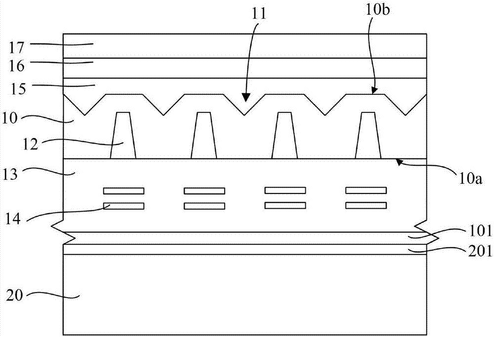
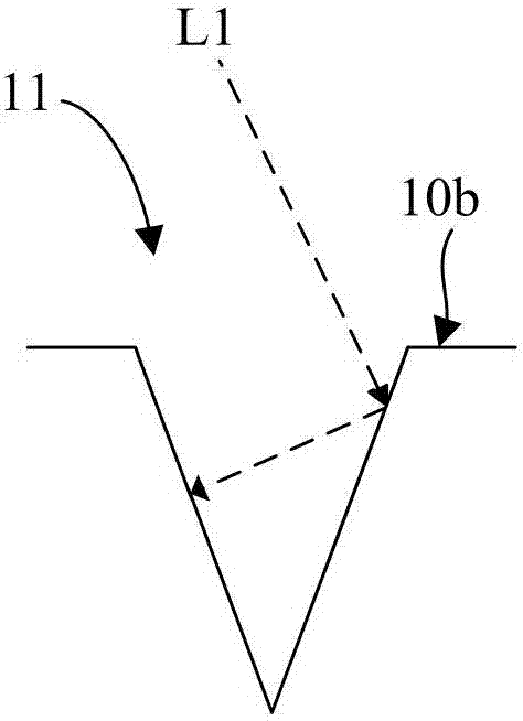
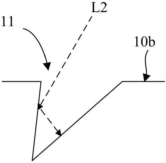
The invention provides a back-illuminated CMOS image sensor and a production method thereof. The back-illuminated CMOS image sensor comprises a first substrate and a second substrate. The front surface of the first substrate is provided with a plurality of pixel units, and the back surface of the first substrate is provided with a plurality of grooves. Each of the grooves is provided with at least one side wall inclined with respect to the back surface of the first substrate. The second substrate is bonded with the first substrate in the front surface direction of the first substrate. The invention also provides the production method of the back-illuminated CMOS image sensor. By disposing the grooves in the back surface of the first substrate, light reflection loss of incident light on the back surface of the first substrate is reduced, and the quantum efficiency of the back-illuminated CMOS image sensor is improved.

Description

technical field [0001] The invention relates to the field of image sensors, in particular to a back-illuminated CMOS image sensor and a manufacturing method thereof. Background technique [0002] Integrated circuit technology has brought about tremendous changes in many fields such as computers, control systems, communications, and images. In the image field, the image sensor is an important part of the digital camera. Image sensors can be divided into CCD (Charge Coupled Device, Charge Coupled Device) image sensors and CMOS (Complementary Metal Oxide Semiconductor, complementary metal-oxide-semiconductor) image sensors according to the difference between photosensitive elements and photosensitive principles. Compared with CCD image sensors, CMOS image sensors can better meet users' increasing quality requirements for image sensors in various applications, such as more flexible image capture, higher sensitivity, wider dynamic range, higher resolution, lower power consumpti...

Claims


Application Information

Patent Timeline
Patent Type & Authority Applications(China)
IPC IPC(8): H01L27/146
CPCH01L27/14629H01L27/14632H01L27/14634H01L27/1464H01L27/14685H01L27/14687H01L27/1469H01L27/14621H01L27/14627H01L27/14636
Inventor 刘艳云董金文付洋朱继锋
Owner WUHAN XINXIN SEMICON MFG CO LTD
Learn More