
Eureka
For R&D, Eureka makes reading and utilizing patents & technical documents easy.
Eureka AIR
Designed for self-driven R&D workflows. Generate viable solutions, solve complex R&D challenges, empower your innovation with AI.

Eureka Materials
Designed for material experts only. Revolutionize your material R&D, from search, analyze, to developing new materials.

TechResearch
Generate reliable direction feasibility study reports for your R&D in just a few steps.

TechSeek
Discover and master advanced knowledge NOW. Basics, ideas, possibilities, all at once.

TechMind
As an expert in R&D Theories, TechMind can generates customized viable solutions instantly.

TechRisk
Analyze your overall solution with one click, know your potential R&D risks in advance.

TechMonitor
Get weekly tech updates, stay abreast of the latest tech innovations and key insights.
Display substrate, manufacturing method thereof, and display device
A technology for display substrates and display areas, applied in instruments, nonlinear optics, optics, etc., can solve the problems of liquid crystal leakage, affecting the cutting process, and high scrap rate, and achieve the effect of improving yield
- Summary
- Abstract
- Description
- Claims
- Application Information
AI Technical Summary
Problems solved by technology
Method used
Image

Examples
Embodiment Construction
[0028] In order to make the object, technical solution and advantages of the present invention clearer, the implementation manner of the present invention will be further described in detail below in conjunction with the accompanying drawings.
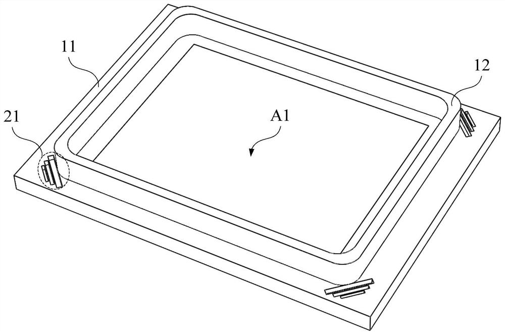
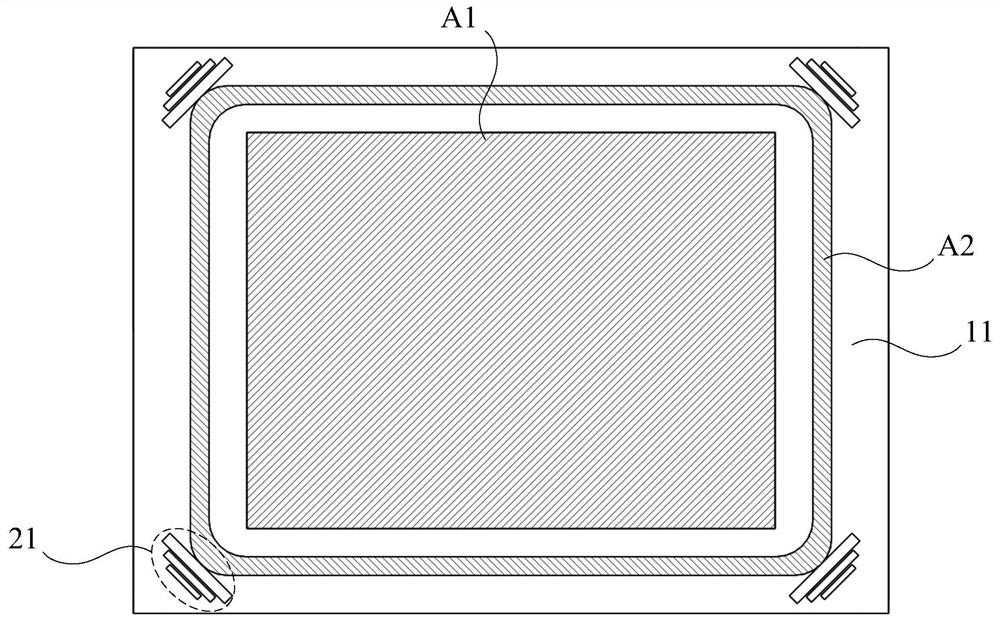
[0029] figure 1 It is a three-dimensional structural schematic diagram of a frame glue part of a display device in an embodiment of the present invention. see figure 1 , the display device includes a display substrate 11 and a sealant 12 arranged on the display substrate 11; in order to make the graphics clear and clear, other parts of the display device and some structural details of the display substrate 11 and the sealant 12 are not shown in figure 1 shown in . It should be noted that the above-mentioned display device can be any product or component with a display function such as a display panel, a mobile phone, a tablet computer, a TV, a monitor, a notebook computer, a digital photo frame, or a navigator; the above-mentioned di...
PUM
 Abstract
Description
Claims
Application Information
 - R&D Engineer
- R&D Manager
- IP Professional
- Industry Leading Data Capabilities
- Powerful AI technology
- Patent DNA Extraction
Browse by: Latest US Patents, China's latest patents, Technical Efficacy Thesaurus, Application Domain, Technology Topic, Popular Technical Reports.
© 2024 PatSnap. All rights reserved.Legal|Privacy policy|Modern Slavery Act Transparency Statement|Sitemap|About US| Contact US: help@patsnap.com