Display panel, preparation method thereof and display device

A display panel and display area technology, which is applied in semiconductor/solid-state device manufacturing, electrical components, electrical solid-state devices, etc., can solve the problems of OLED display device packaging and display performance damage, complex structure, poor packaging coverage, etc., to improve packaging. Quality and display performance, the effect of reducing bezels

Active Publication Date: 2017-09-19
BOE TECH GRP CO LTD
View PDF6 Cites 73 Cited by
  • Summary
  • Abstract
  • Description
  • Claims
  • Application Information

AI Technical Summary

Problems solved by technology

The packaging area includes the effective display area and the non-display area. The non-display area is arranged with structures such as circuit leads and driving circuits. Display area, i.e. the edge of the package is close to the edge of the non-display area of ​​the device
[0005] After the OLED display device is packaged, it needs to be cut from the mother board. During the cutting process, due to the internal stress of the inorganic packaging film and other inorganic insulating layers extending to the edge of the non-display area in the device, the non-display area of ​​the device is located in the cutting area. The inorganic packaging film and other inorganic insulating layers near the line are prone to cracks during cutting, and the cracks are easy to spread along the inorganic packaging film and other inorganic insulating layers to the display area, resulting in damage to the packaging and display performance of OLED display devices

Method used


Image

  • Display panel, preparation method thereof and display device
  • Display panel, preparation method thereof and display device
  • Display panel, preparation method thereof and display device

Examples


Embodiment 1

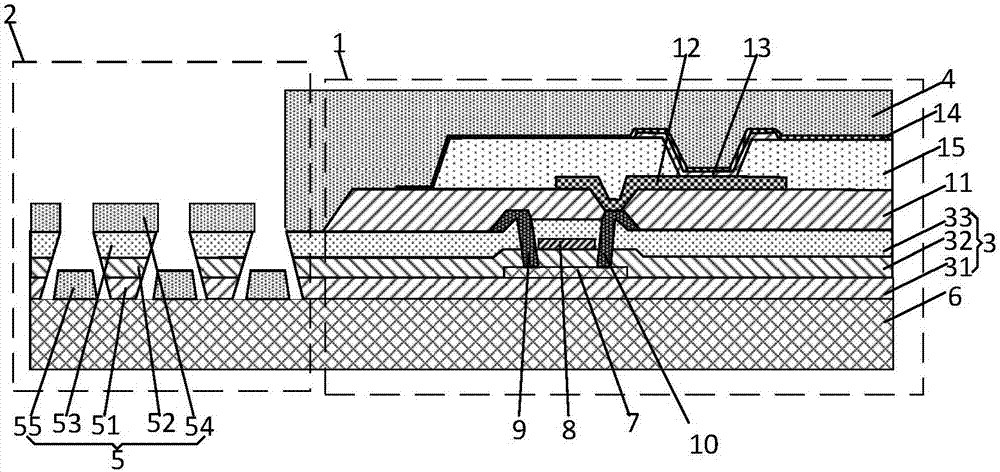
[0060] This embodiment provides a display panel, such as figure 1 and figure 2 As shown, including the display area 1 and the frame area 2, the display area 1 and the frame area 2 are both provided with an inorganic insulating layer 3 and an inorganic encapsulation layer 4, and both the inorganic insulating layer 3 and the inorganic encapsulation layer 4 of the frame area 2 are formed with discontinuities The structure 5, the discontinuous structure 5 can block the crack propagation in the inorganic insulating layer 3 and the inorganic encapsulation layer 4 .

[0061] By forming the discontinuous structure 5 in the inorganic insulating layer 3 and the inorganic encapsulation layer 4 of the frame area 2, when the display panel is cut from the motherboard, the discontinuous structure 5 can block the inorganic insulating layer 3 and the inorganic encapsulation layer near the cutting line. The propagation path of the cracks generated in the layer 4, so that the cracks generated ...

Embodiment 2

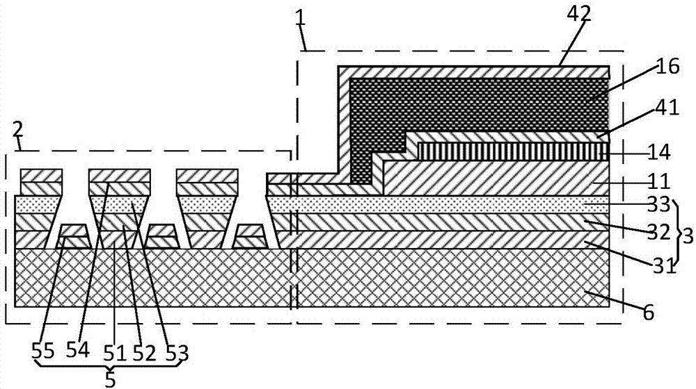
[0081] This embodiment provides a display panel, which is different from that in Embodiment 1, such as image 3 As shown, the discontinuous structure 5 includes a second inverted truncated cone structure 52 and a third inverted truncated cone structure 53 respectively formed in the gate insulating layer 32 and the passivation layer 33, the second inverted truncated cone structure 52 and the gate insulating layer 32 The other parts are spaced apart from each other; the third inverted truncated cone structure 53 is spaced apart from other parts of the passivation layer 33; the second inverted truncated cone structure 52 and the third inverted truncated cone structure 53 correspond to each other and overlap each other to form an inverted truncated cone shape the whole frame. The discontinuous structure 5 also includes a first structure 54 and a second structure 55 formed in the inorganic encapsulation layer 4, the first structure 54 is correspondingly arranged above the third inv...

Embodiment 3

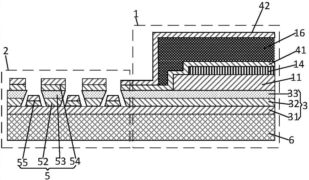
[0091] This embodiment provides a display panel, which is different from Embodiment 1-2, such as Figure 4 As shown, the inorganic insulating layer 3 also includes a pixel definition layer 15, a part of the pixel definition layer 15 is arranged in the display area 1, and the other part is arranged in the frame area 2; in the frame area 2, the pixel definition layer 15 is overlaid on the passivation layer 33 .

[0092] In this embodiment, the discontinuous structure 5 further includes a fourth inverted frustum structure 56 formed in the pixel defining layer 15 , and the fourth inverted frustum structure 56 is spaced apart from other parts of the pixel defining layer 15 . The fourth inverted frustum structure 56 corresponds to the first inverted frustum structure 51 , the second inverted frustum structure 52 and the third inverted frustum structure 53 and overlaps each other to form an inverted frustum-like integral structure. The first structure 54 is correspondingly located o...


PUM


Abstract

The present invention provides a display panel, a preparation method thereof and a display device. The display panel comprises a display area and a frame area. The display area and the frame area are respectively provided with an inorganic insulating layer and an inorganic encapsulating layer. A discontinuity structure is arranged inside each of the inorganic insulating layer and the inorganic encapsulating layer of the frame area, and the discontinuity structure can block the crack propagation in the inorganic insulating layer and the inorganic encapsulating layer. The discontinuity structure of the display panel is capable of blocking the propagation path of cracks in the inorganic insulating layer and the inorganic encapsulating layer and generated near a cutting line. Therefore, cracks in the inorganic insulating layer and the inorganic encapsulating layer and generated near the cutting line cannot be extended to the display area of the display panel. As a result, the display performance of the display panel is not damaged. Meanwhile, the narrow frame of the display panel can be realized.

Description

technical field [0001] The present invention relates to the field of display technology, in particular, to a display panel, a manufacturing method thereof, and a display device. Background technique [0002] OLED (organic electroluminescent) display device, through the organic light-emitting material layer self-luminous display, does not need a backlight source, it has faster response speed, larger viewing angle, higher contrast, lighter weight, low power consumption It is considered to be the flat panel display device with the most development potential due to its flexible use and other characteristics. At the same time, OLED display devices can be made into flexible display devices. [0003] However, the lifespan of OLED display devices restricts the pace of its industrialization. When the OLED display device is working, electrons are injected from the cathode to the transport layer. In order to increase the number of injected carriers and improve luminous efficiency, the...

Claims


Application Information

Patent Timeline
Patent Type & Authority Applications(China)
IPC IPC(8): H01L51/52H01L27/32H01L51/56
CPCH10K59/12H10K50/844H10K71/00
Inventor 孙韬张嵩
Owner BOE TECH GRP CO LTD
Why Eureka
Try Eureka