Display panel, manufacturing method thereof, and display device
A display panel and display area technology, applied in semiconductor/solid-state device manufacturing, semiconductor devices, electrical components, etc., can solve problems such as complex structure, OLED display device packaging and display performance damage, poor packaging coverage, etc., to reduce the border , Improve packaging quality and display performance
- Summary
- Abstract
- Description
- Claims
- Application Information
AI Technical Summary
Problems solved by technology
Method used
Image
Examples
Embodiment 1
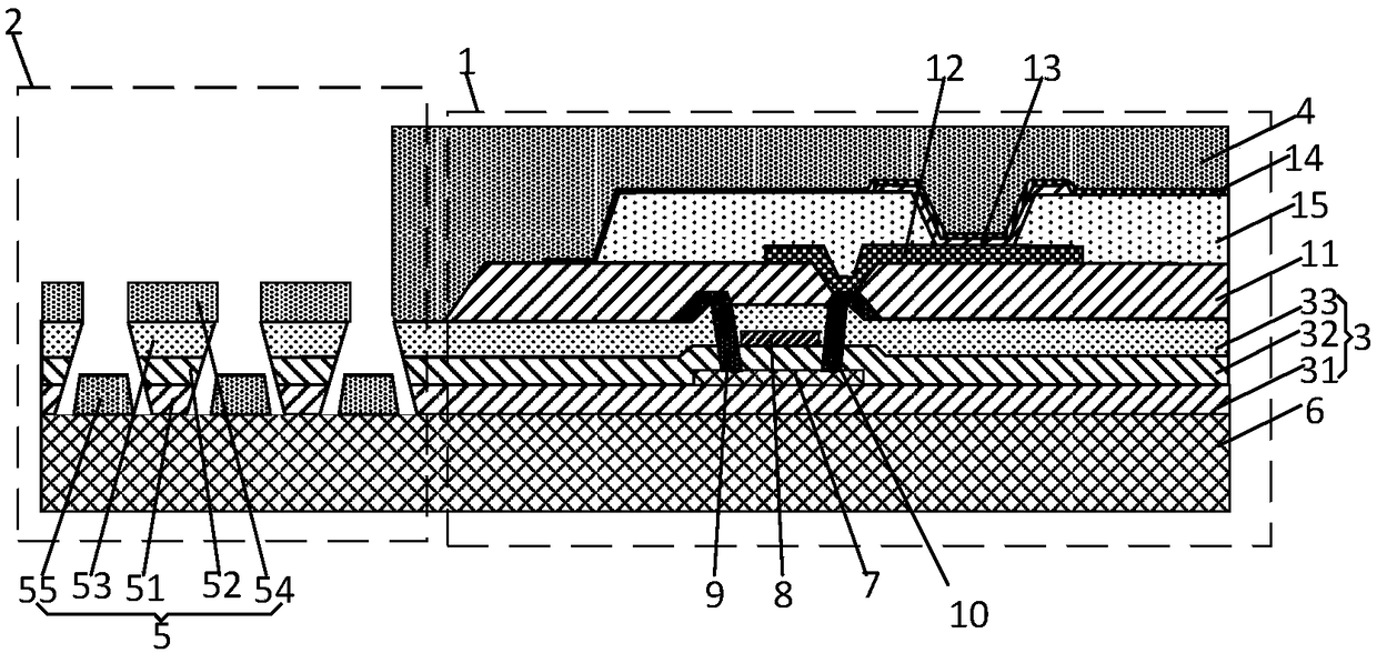
[0060] This embodiment provides a display panel, such as figure 1 with figure 2 As shown, including the display area 1 and the frame area 2, the display area 1 and the frame area 2 are both provided with an inorganic insulating layer 3 and an inorganic encapsulation layer 4, and both the inorganic insulating layer 3 and the inorganic encapsulation layer 4 of the frame area 2 are formed with discontinuities The structure 5, the discontinuous structure 5 can block the crack propagation in the inorganic insulating layer 3 and the inorganic encapsulation layer 4 .
[0061] By forming the discontinuous structure 5 in the inorganic insulating layer 3 and the inorganic encapsulation layer 4 of the frame area 2, when the display panel is cut from the motherboard, the discontinuous structure 5 can block the inorganic insulating layer 3 and the inorganic encapsulation layer near the cutting line. The propagation path of the cracks generated in the layer 4, so that the cracks generated...
Embodiment 2
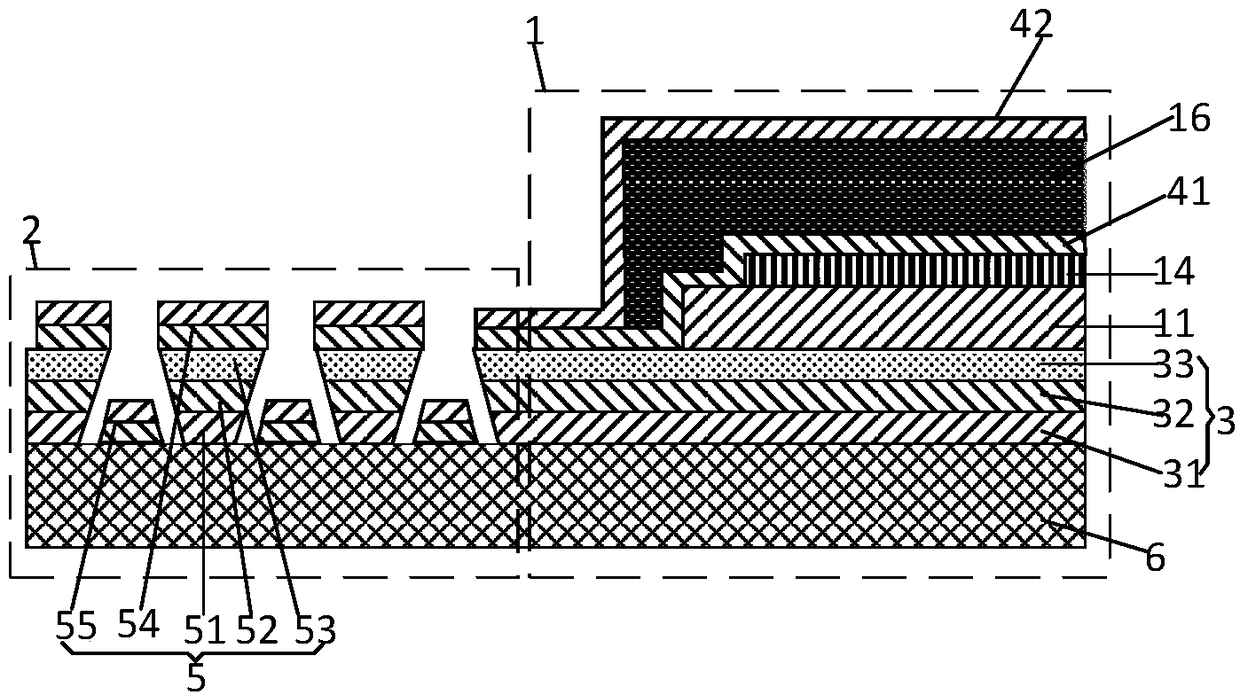
[0081] This embodiment provides a display panel, which is different from that in Embodiment 1, such as image 3 As shown, the discontinuous structure 5 includes a second inverted truncated cone structure 52 and a third inverted truncated cone structure 53 respectively formed in the gate insulating layer 32 and the passivation layer 33, the second inverted truncated cone structure 52 and the gate insulating layer 32 The other parts are spaced apart from each other; the third inverted truncated cone structure 53 is spaced apart from other parts of the passivation layer 33; the second inverted truncated cone structure 52 and the third inverted truncated cone structure 53 correspond to each other and overlap each other to form an inverted truncated cone shape the whole frame. The discontinuous structure 5 also includes a first structure 54 and a second structure 55 formed in the inorganic encapsulation layer 4, the first structure 54 is correspondingly arranged above the third inv...
Embodiment 3
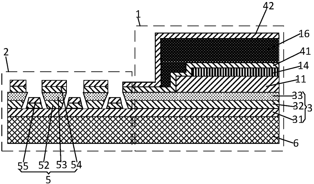
[0091] This embodiment provides a display panel, which is different from Embodiment 1-2, such as Figure 4 As shown, the inorganic insulating layer 3 also includes a pixel defining layer, a part of the pixel defining layer is disposed in the display area 1 , and the other part is disposed in the frame area 2 ; in the frame area 2 , the pixel defining layer is overlaid on the passivation layer 33 .
[0092] In this embodiment, the discontinuous structure 5 further includes a fourth inverted frustum structure 56 formed in the pixel defining layer, and the fourth inverted frustum structure 56 is spaced apart from other parts of the pixel defining layer. The fourth inverted frustum structure 56 corresponds to the first inverted frustum structure 51 , the second inverted frustum structure 52 and the third inverted frustum structure 53 and overlaps each other to form an inverted frustum-like integral structure. The first structure 54 is correspondingly located on the fourth inverted...
PUM
 Abstract
Description
Claims
Application Information


