Array substrate and display panel

An array substrate and display panel technology, applied in static indicators, nonlinear optics, instruments, etc., can solve the problems of screen whitening and residual image, large voltage difference between pixel electrode and common electrode, etc., to avoid whitening and residual image. Effect

Inactive Publication Date: 2017-09-22
SHENZHEN CHINA STAR OPTOELECTRONICS SEMICON DISPLAY TECH CO LTD
View PDF5 Cites 10 Cited by
  • Summary
  • Abstract
  • Description
  • Claims
  • Application Information

AI Technical Summary

Problems solved by technology

[0004] The present invention provides an array substrate and a display panel to solve the technical problems in the prior art that the voltage difference between the pixel electrode and the common electrode is too large when the liquid crystal display is turned off, and the screen has white afterimages

Method used


Image

  • Array substrate and display panel
  • Array substrate and display panel
  • Array substrate and display panel

Examples


Embodiment Construction

[0017] The following will clearly and completely describe the technical solutions in the embodiments of the present invention with reference to the accompanying drawings in the embodiments of the present invention. Obviously, the described embodiments are only some, not all, embodiments of the present invention. Based on the embodiments of the present invention, all other embodiments obtained by persons of ordinary skill in the art without making creative efforts belong to the protection scope of the present invention.

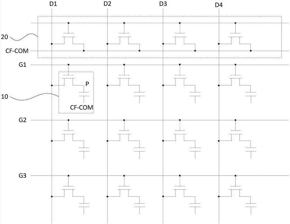
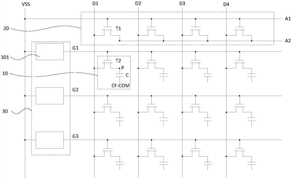
[0018] see figure 1 , an embodiment of the array substrate of the present invention includes:

[0019] A plurality of scanning lines Gn, this embodiment takes the scanning lines G1-G3 as an example for illustration;

[0020] A plurality of data lines Dn, the present embodiment takes the data lines D1-D4 as an example for illustration, and are arranged to cross each other with a plurality of scanning lines Gn, thereby defining a plurality of pixel regions 10; ...


PUM


Abstract

The invention discloses an array substrate and a display panel. The array substrate comprises multiple scanning lines, data lines arranged to be crossed with the scanning lines so as to define multiple pixel areas and a control circuit which is connected with multiple data lines and used for making voltage on the data lines equal to that of a common electrode during shutdown and making voltage of pixel electrodes in the pixel areas equal to that of the data lines. Accordingly, the voltage difference between the pixel electrodes in the pixel areas and the common electrode during shutdown can be balanced, liquid crystals do not deflect, and white ghosting of a screen is avoided.

Description

technical field [0001] The invention relates to the technical field of liquid crystal display, in particular to an array substrate and a display panel. Background technique [0002] Due to its small size, low power consumption, and low radiation, liquid crystal displays occupy a leading position in the field of flat-panel displays. With the development of liquid crystal display technology, high resolution, high contrast, narrow frame, and thinning have become the development trend of liquid crystal displays. GOA (Gate Driver On Array, array substrate line drive) can use the original process of the liquid crystal display panel to manufacture the horizontal scanning drive circuit on the substrate around the display area, so that it can replace the original external IC (Integrated Circuit, integrated circuit) to complete the drive of the horizontal scanning line, which can reduce the process of external IC, reduce the product cost, and make the liquid crystal display panel mor...

Claims


Application Information

Patent Timeline
Patent Type & Authority Applications(China)
IPC IPC(8): G02F1/1362G02F1/1343G02F1/133
CPCG02F1/13306G02F1/134309G02F1/136286
Inventor 石龙强
Owner SHENZHEN CHINA STAR OPTOELECTRONICS SEMICON DISPLAY TECH CO LTD
Why Eureka
Try Eureka