
Flexible substrate packaging structure and packaging method thereof

A technology of flexible substrates and packaging structures, applied in the direction of electrical components, electrical solid devices, circuits, etc., can solve the problems of long production process, complicated production process, and multiple supply chains, and achieve the effect of reducing intermediate supply chains and simplifying the production process

Active Publication Date: 2017-09-26
NAT CENT FOR ADVANCED PACKAGING
View PDF4 Cites 5 Cited by
  • Summary
  • Abstract
  • Description
  • Claims
  • Application Information

AI Technical Summary

Problems solved by technology

However, there will be problems such as a relatively long production process and too many supply chains.
In addition, in the prior art, in order to bond the chip and the flexible substrate smoothly, it is necessary to make corresponding solder balls on the chip in advance, and the manufacturing process is complicated and the manufacturing cost is relatively high.

Method used


Image

  • Flexible substrate packaging structure and packaging method thereof
  • Flexible substrate packaging structure and packaging method thereof
  • Flexible substrate packaging structure and packaging method thereof

Examples


Embodiment Construction

[0035] The present invention will be further described in detail below in conjunction with the accompanying drawings and embodiments. It should be understood that the specific embodiments described here are only used to explain the present invention, but not to limit the present invention. In addition, it should be noted that, for the convenience of description, only some structures related to the present invention are shown in the drawings but not all structures.

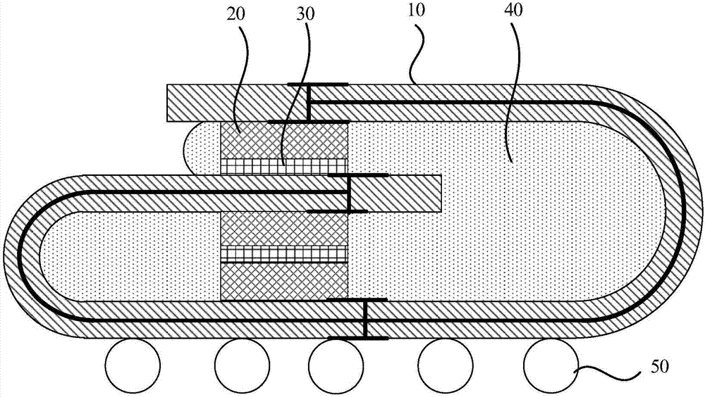
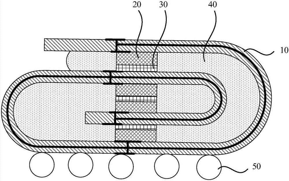
[0036] figure 1 A schematic diagram of a flexible packaging structure provided for an embodiment of the present invention, such as figure 1 As shown, the flexible substrate packaging structure provided by the embodiment of the present invention includes: a flexible substrate 10 , a plurality of chips 20 and a silicone material 40 . Wherein, a plurality of chips 20 are formed on the flexible substrate 40, an adhesive layer 30 is arranged on the side of the chips 20 facing away from the flexible substrate 10, and t...


PUM


Abstract

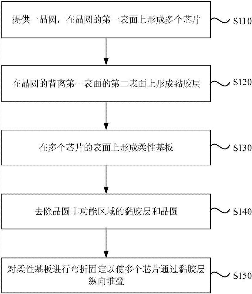
An embodiment of the invention discloses a flexible substrate packaging structure and a packaging method thereof. The flexible packaging structure comprises a flexible substrate and a plurality of chips formed on the flexible substrate, wherein an adhesive layer is arranged on one surface, deviating from the flexible substrate, of each chip, and the plurality of chips are laminated longitudinally after being bent by the flexible substrate and fixed by the adhesive layers. With the adoption of the flexible substrate packaging structure and the packaging method thereof, the production procedure of the flexible substrate packaging structure can be simplified.

Description

technical field [0001] Embodiments of the present invention relate to substrate packaging technology in the microelectronics industry, and in particular to a flexible substrate packaging structure and a packaging method thereof. Background technique [0002] At present, the development trend of semiconductor packaging is more and more towards high frequency, multi-chip module (MCM), and high IO pins. 3D ICs that integrate different chip stacks will become the mainstream development trend. The market share of system-integrated (SiP) packaging and stacked packaging (PiP, PoP) is also increasing year by year, and 2.5D / 3D TSV technology is also in the stage of mass production. . Due to the limitation of package dimensions, it is necessary to put different functional modules (such as chips) in one package. Stacking chips after folding is a major trend in technology development. [0003] Existing mass production solutions mostly use chips and flexible substrates to be designed,...

Claims


Application Information

Patent Timeline
Patent Type & Authority Applications(China)
IPC IPC(8): H01L25/065H01L21/50
CPCH01L25/0657H01L21/50H01L2225/06555
Inventor 徐健
Owner NAT CENT FOR ADVANCED PACKAGING
Learn More