

In-mold anti-counterfeiting label and preparation method thereof
A technology of anti-counterfeiting labels and substrate layers, which is applied in the field of anti-counterfeiting labels in film and its preparation, can solve the problem that the coding on the reverse side cannot be combined with the carrier, etc., and achieves the effect of reducing the deviation of the positive and negative positions and improving the production efficiency.
- Summary
- Abstract
- Description
- Claims
- Application Information
AI Technical Summary
Problems solved by technology
Method used
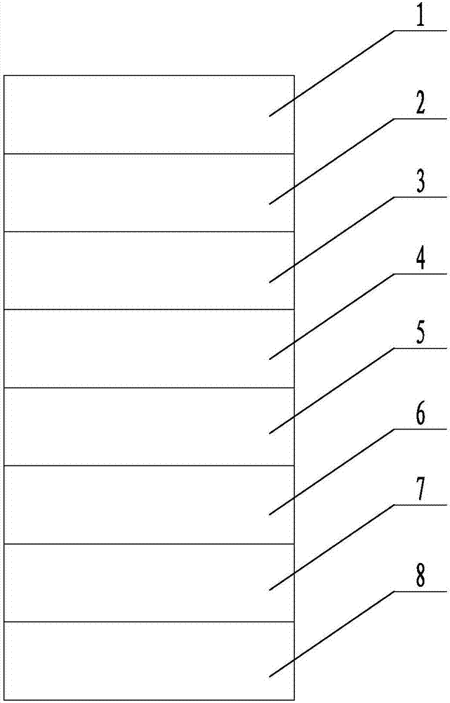
Image

Examples
Embodiment 1
[0032] Customer orders (1 million)
[0033] (1) Selecting a first substrate layer with a thickness of 8 μm;
[0034] (2) The first information layer and the second information layer are given on the first substrate layer by means of front and back printing;
[0035] (3) Use two-component glue to combine the first substrate layer and the second substrate layer together, and cure for 24 hours;
[0036] (4) protective layer protection is carried out on the surface of the first substrate layer;
[0037] (5) Use a coating machine to coat static elimination liquid on the protective layer;
[0038] (6) Coating meltable glue on the second substrate layer;
[0039] (7) Die-cutting: Use an automatic die-cutting machine to cut into individual films and paste anti-counterfeiting labels inside.
Embodiment 2
[0041] Customer orders (2 million)
[0042] (1) Selecting a first substrate layer with a thickness of 50 μm;
[0043] (2) The first information layer and the second information layer are given on the first substrate layer by means of front and back printing;
[0044] (3) The first substrate layer and the second substrate layer are composited together using a two-component adhesive, and cured for 36 hours;
[0045] (4) protective layer protection is carried out on the surface of the first substrate layer;
[0046] (5) Use a coating machine to coat static elimination liquid on the protective layer;
[0047] (6) Coating meltable glue on the second substrate layer;
[0048] (7) Die-cutting: Use an automatic die-cutting machine to cut into individual films and paste anti-counterfeiting labels inside.
Embodiment 3
[0050] Customer orders (3 million)
[0051] (1) Selecting a first substrate layer with a thickness of 120 μm;
[0052] (2) The first information layer and the second information layer are given on the first substrate layer by means of front and back printing;
[0053] (3) The first substrate layer and the second substrate layer are composited together using a two-component adhesive, and cured for 48 hours;
[0054] (4) protective layer protection is carried out on the surface of the first substrate layer;
[0055] (5) Use a coating machine to coat static elimination liquid on the protective layer;
[0056] (6) Coating meltable glue on the second substrate layer;
[0057] (7) Die-cutting: Use an automatic die-cutting machine to cut into individual films and paste anti-counterfeiting labels inside.
PUM
| Property | Measurement | Unit |
|---|---|---|
| Thickness | aaaaa | aaaaa |
| Thickness | aaaaa | aaaaa |
| Thickness | aaaaa | aaaaa |
Abstract
Description
Claims
Application Information