level conversion circuit

A technology for converting circuits and levels, applied in logic circuits, logic circuit connection/interface layout, electrical components, etc., can solve the problems of increasing circuit complexity, circuit area, low circuit conversion speed, large circuit area, etc., to achieve easy implementation and integration, fast circuit conversion speed, and simple circuit structure

Active Publication Date: 2020-11-17
HUNAN GOKE MICROELECTRONICS
View PDF10 Cites 0 Cited by
  • Summary
  • Abstract
  • Description
  • Claims
  • Application Information

AI Technical Summary

Problems solved by technology

[0002] Existing level conversion circuits, such as a single-ended negative voltage level conversion circuit structure described in the patent US6483366B2, due to the large output voltage span, in order to prevent the device from being broken down, high-voltage tubes or other auxiliary circuits must be used, so that The circuit area is large, which increases the cost; and the circuit conversion speed is low and the power consumption is high
[0003] Another example is a level conversion circuit described in patent CN 104242909 A. In order to realize the conversion from positive voltage to negative voltage, the level conversion circuit needs to solve the withstand voltage problem of the device through the auxiliary circuit of N well conversion structure, which increases the circuit The complexity and area of ​​the circuit

Method used


Image

  • level conversion circuit

Examples


Embodiment Construction

[0026] The following will clearly and completely describe the technical solutions in the embodiments of the present invention. Obviously, the described embodiments are only some of the embodiments of the present invention, rather than all the embodiments. Based on the embodiments of the present invention, all other embodiments obtained by persons of ordinary skill in the art without making creative efforts belong to the protection scope of the present invention.

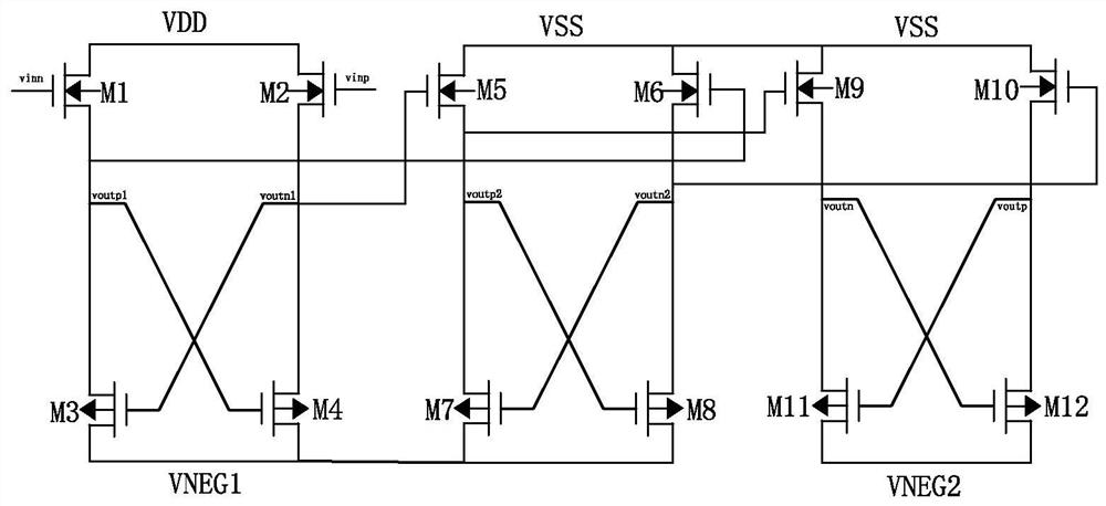
[0027] see figure 1 , is a circuit diagram of the level conversion circuit of the present invention. The present invention provides a level conversion circuit, the level conversion circuit includes:

[0028] MOS tube M1, MOS tube M2, MOS tube M3, MOS tube M4, MOS tube M5, MOS tube M6, MOS tube M7, MOS tube M8, MOS tube M9, MOS tube M10, MOS tube M11 and MOS tube M12. Wherein, the MOS transistor M1, the MOS transistor M2, the MOS transistor M5, the MOS transistor M6, the MOS transistor M9, and the MOS transistor M10...


PUM


Abstract

The invention provides a level conversion circuit. The level conversion circuit comprises an MOS tube M1, an MOS tube M2, an MOS tube M3, an MOS tube M4, an MOS tube M5, an MOS tube M6, an MOS tube M7, an MOS tube M8, an MOS tube M9, an MOS tube M10, an MOS tube M11 and an MOS tube M12. Compared with the prior art, the level conversion circuit provided by the invention solves the voltage-withstanding problem during the negative-voltage level conversion process. Meanwhile, the level conversion circuit is high in circuit conversion speed, low in power consumption, simple in circuit structure, small in area, low in cost and easy to implement and integrate.

Description

technical field [0001] The invention relates to the technical field of level conversion, in particular to a level conversion circuit. Background technique [0002] Existing level conversion circuits, such as a single-ended negative voltage level conversion circuit structure described in the patent US6483366B2, due to the large output voltage span, in order to prevent the device from being broken down, high-voltage tubes or other auxiliary circuits must be used, so that The circuit area is large, which increases the cost; moreover, the switching speed of the circuit is low, and the power consumption is high. [0003] Another example is a level conversion circuit described in patent CN 104242909 A. In order to realize the conversion from positive voltage to negative voltage, the level conversion circuit needs to solve the withstand voltage problem of the device through an auxiliary circuit of N-well conversion structure, which increases the circuit complexity and circuit area...

Claims


Application Information

Patent Timeline
Patent Type & Authority Patents(China)
IPC IPC(8): H03K19/0185
CPCH03K19/018507
Inventor 陈婷谢俊杰姜黎喻彪周倩
Owner HUNAN GOKE MICROELECTRONICS
Why Eureka
Try Eureka