A level conversion circuit

A technology for converting circuits and levels, applied in the directions of logic circuits, logic circuit interface devices, logic circuit connection/interface layout, etc., can solve problems such as the inability to solve the withstand voltage problem, the inability of NMOS transistors N1 and N2 to conduct, and achieve the realization of The effect of wide power supply voltage, realization of conversion, and avoidance of withstand voltage problems

Active Publication Date: 2022-07-29
CHENGDU ANALOG CIRCUIT TECH INC
View PDF19 Cites 0 Cited by
  • Summary
  • Abstract
  • Description
  • Claims
  • Application Information

AI Technical Summary

Problems solved by technology

[0003] However, with the continuous improvement of application requirements, some applications require devices to support low voltage of 0.9V, or even lower than 0.9V, figure 1 The NMOS transistors N1 and N2 in the circuit structure will not be able to conduct
If will figure 1 If the NMOS tube in the circuit structure is replaced by a low-voltage tube, it will face the problem of its withstand voltage that cannot be solved.

Method used


Image

  • A level conversion circuit
  • A level conversion circuit

Examples


Embodiment Construction

[0018] It should be understood that the specific embodiments described herein are only used to explain the present invention, but not to limit the present invention.

[0019] The present invention will be further described below with reference to the accompanying drawings.

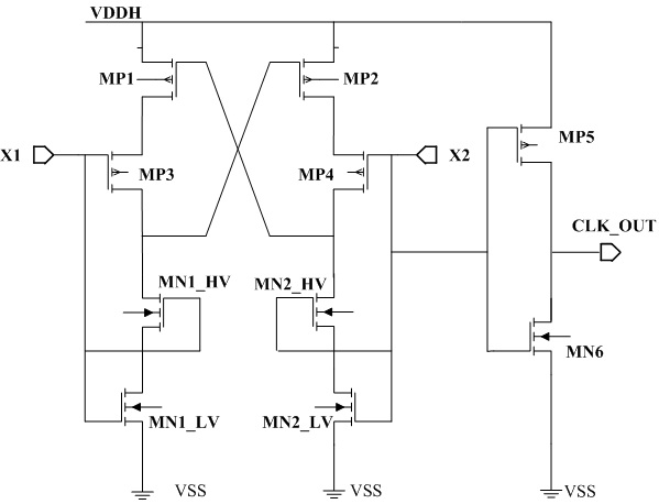
[0020] A level shifting circuit such as figure 2 As shown, it includes a first field effect transistor MP1 and a second field effect transistor MP2 connected to the power supply voltage VDDH, a third field effect transistor MP3 connected to the first input terminal X1, a first high voltage native transistor MN1_HV and a first low voltage field effect transistor. Effect transistor MN1_LV, the fourth field effect transistor MP4 connected to the second input terminal X2, the second high voltage native transistor MN2_HV and the second low voltage field effect transistor MN2_LV, the fourth field effect transistor MP4 and the second high voltage native transistor MN2_HV and the second low voltage field effect ...


PUM


Abstract

The invention discloses a level conversion circuit, which relates to the technical field of integrated circuits. The level conversion circuit includes a first field effect transistor and a second field effect transistor connected to a power supply voltage, a third field effect transistor, a first high-voltage native transistor and a first low-voltage field effect transistor connected to the first input end, connected to the The fourth FET, the second high-voltage native transistor and the second low-voltage FET at the second input end, the fourth FET, the second high-voltage native transistor and the second low-voltage FET are also connected to the circuit output through an inverter terminal; the first field effect transistor is connected to the third field effect transistor, the fourth field effect transistor and the second high voltage native tube; the second field effect transistor is connected to the third field effect transistor, the fourth field effect transistor and the first high voltage native tube tube; the first high-voltage native tube is grounded through the first low-voltage field effect tube, and the second high-voltage native tube is grounded through the second low-voltage field effect tube. The technical scheme of the present invention realizes the conversion of the wide power supply voltage of the circuit.

Description

technical field [0001] The present invention relates to the technical field of integrated circuits, in particular to a level conversion circuit. Background technique [0002] Level shifting circuits are very common in analog circuits and are often used to convert between different levels to boost low voltage signals to high voltage levels. However, with the further reduction of the operating voltage of low-voltage devices, the traditional low-voltage to high-voltage level conversion circuit encounters a bottleneck in a wide power supply range. E.g figure 1 In the traditional structure, the field effect transistors in the circuit are all high voltage tubes. Under normal circumstances, when the input terminals V1 and V2 receive a low-voltage 1.2V clock input, they can output a 3.3V high-voltage clock at the CLK_OUT terminal, and the voltages are all typical values. In other demanding applications, the voltage conversion can exceed ten percent, that is, the maximum level con...

Claims


Application Information

Patent Timeline
Patent Type & Authority Patents(China)
IPC IPC(8): H03K19/0185
CPCH03K19/017509H03K19/018507
Inventor 宋登明
Owner CHENGDU ANALOG CIRCUIT TECH INC
Why Eureka
Try Eureka