A radiation-resistant semiconductor device terminal structure

A terminal structure and semiconductor technology, applied in the direction of semiconductor devices, electrical components, circuits, etc., can solve the problems of degradation of electrical characteristics in the active area, failure to slow down the degradation of electrical characteristics in the terminal area, and the impact of the terminal area of ​​​​the device, so as to solve the terminal withstand voltage problems, improving the surface electric field, and avoiding the effects of breakdown

Active Publication Date: 2020-12-18
UNIV OF ELECTRONICS SCI & TECH OF CHINA
View PDF5 Cites 0 Cited by
  • Summary
  • Abstract
  • Description
  • Claims
  • Application Information

AI Technical Summary

Problems solved by technology

Radiation effects not only degrade the electrical properties of the active area, but also affect the terminal area of ​​the device
The traditional reinforcement and anti-radiation reinforcement method only strengthens the active area, and cannot slow down the degradation of electrical characteristics caused by the radiation effect in the terminal area

Method used


Image

  • A radiation-resistant semiconductor device terminal structure
  • A radiation-resistant semiconductor device terminal structure
  • A radiation-resistant semiconductor device terminal structure

Examples


Embodiment 1

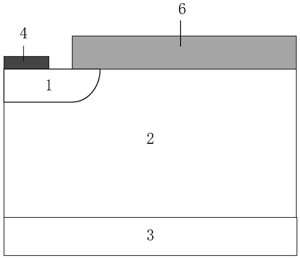
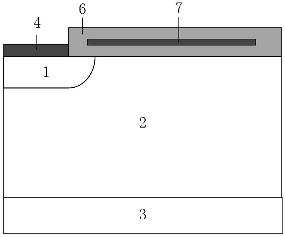
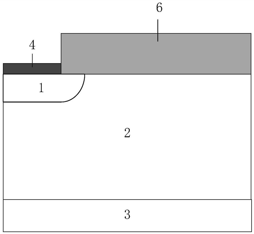
[0033] Such as figure 2 As shown, it includes a first conductivity type semiconductor substrate 3, a first conductivity type semiconductor drift region 2 located on the upper surface of the first conductivity type semiconductor substrate 3, and a first conductivity type semiconductor drift region 2 formed in the first conductivity type semiconductor drift region 2. Cell region extension well 1 of two conductivity types; the upper surface of semiconductor drift region 2 of the first conductivity type and part of the upper surface of cell region extension well 1 of the second conductivity type have an insulating layer 6, and the first metal electrode 4 is located on Part of the upper surface of the cell region of the second conductivity type extending well 1, the polysilicon strip 7 is located on the upper surface of the semiconductor drift region 2 of the first conductivity type and the insulation of part of the upper surface of the cell region of the second conductivity type e...

Embodiment 2

[0048] Such as Figure 4 As shown, the difference between this embodiment and Embodiment 1 is that the polysilicon strips 7 are intermittently distributed in the lateral direction, and this structure will further improve the radiation resistance of the terminal. A plurality of discontinuous polysilicon strips will modulate the terminal electric field in a non-radiative state and improve the withstand voltage of the device.

[0049] As a preferred manner, the distances between the discontinuous portions of the polysilicon strip 7 in the lateral direction and the upper surface of the drift region 2 of the semiconductor of the first conductivity type are different.

Embodiment 3

[0051] Figure 5An application example of this embodiment to a planar gate is given, indicating that the present invention can be applied to various vertical device structures.

[0052] In addition, the coverage, width and number of polysilicon strips can be adjusted according to the process conditions. Multiple polysilicon strips or thickened polysilicon strips will improve the radiation resistance of the terminal.


PUM


Abstract

The present invention provides a terminal structure of a radiation-resistant semiconductor device, comprising a semiconductor substrate of a first conductivity type, a drift region of a semiconductor of the first conductivity type, an extended well of a cell region of a second conductivity type, an insulating layer, a first metal electrode, For the polysilicon strip, the invention can effectively suppress the phenomenon of charge accumulation in the terminal oxide layer due to radiation, and prevent device breakdown due to charge accumulation in the terminal oxide layer. The surface electric field of the device terminal after radiation can be improved, and the breakdown voltage of the device terminal can be improved. The invention is simple, feasible and low in process difficulty, and can well solve the problem of terminal withstand voltage after radiation.

Description

technical field [0001] The invention belongs to the technical field of power semiconductor devices, and in particular relates to a terminal structure of a radiation-resistant semiconductor device. Background technique [0002] The ideal device breakdown voltage refers to the case where the PN junction is a planar junction. Due to the influence of the junction termination effect, the device breakdown voltage is restricted by the breakdown voltage of the terminal region. Radiation effects not only degrade the electrical properties of the active region, but also affect the termination region of the device. The traditional anti-radiation reinforcement method only strengthens the active area, and cannot slow down the degradation of electrical characteristics caused by the radiation effect in the terminal area. Contents of the invention [0003] The purpose of the present invention is to solve the above problems and propose a radiation-resistant power device terminal structure ...

Claims


Application Information

Patent Timeline
Patent Type & Authority Patents(China)
IPC IPC(8): H01L29/06
Inventor 周锌赵凯马阔乔明张波
Owner UNIV OF ELECTRONICS SCI & TECH OF CHINA
Why Eureka
Try Eureka