Liquid crystal display panel binding method and structure

A liquid crystal display panel, bonding technology, applied in static indicators, nonlinear optics, optics, etc., can solve the problem of difficult to achieve narrow border display, achieve narrow border display and narrow border splicing display, improve display effect, Realize the effect of narrow border display

Active Publication Date: 2017-11-28
TCL CHINA STAR OPTOELECTRONICS TECH CO LTD
View PDF12 Cites 38 Cited by
  • Summary
  • Abstract
  • Description
  • Claims
  • Application Information

AI Technical Summary

Problems solved by technology

Figure 5 Schematic diagram of bonding structure for existing LCD panels, such as Figure 5 As shown, in the bonding structure of the liquid crystal display panel, the edge of the upper surface of the TFT substrate 310 is provided with a bonding area 315, and metal leads 600 are distributed in the bonding area 315, and the metal leads 600 pass through the anisotropic conductive adhesive film (Anisotropi

Method used


Image

  • Liquid crystal display panel binding method and structure
  • Liquid crystal display panel binding method and structure
  • Liquid crystal display panel binding method and structure

Examples


Embodiment Construction

[0047] In order to further illustrate the technical means adopted by the present invention and its effects, the following describes in detail in conjunction with preferred embodiments of the present invention and accompanying drawings.

[0048] see Image 6 , the present invention provides the bonding method of the first liquid crystal display panel, comprising the following steps:

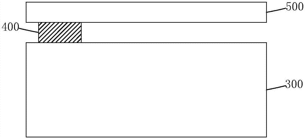
[0049] Step 1, such as Figure 8 and Figure 9 As shown, a liquid crystal display panel 90 is provided, and the liquid crystal display panel 90 includes a CF substrate 10 and a TFT substrate 20 arranged oppositely, and is arranged between the CF substrate 10 and the TFT substrate 20 for connecting the CF substrate 10 and the TFT substrate 20 to form a sealant 30 for sealing the space; the upper surface 21 of the TFT substrate 20 close to the CF substrate 10 is provided with a lead 40 .

[0050] Specifically, such as Figure 8 and Figure 9 As shown, the lead wire 40 includes a part located in...


PUM


Abstract

The invention provides a liquid crystal display panel binding method and structure. The liquid crystal display panel binding method is that fusion metal material or conductive glue material is applied to the side surface and the upper surface of a TFT substrate to form a conductive pattern connected with a lead wire; and then conductive pattern and a flip-chip thin film can be bond when anisotropic conductive adhesive film is arranged on the side surface of the TFT substrate. The process is simple; a binding area is arranged on the side surface of the TFT substrate, so compared with a binding method of arranging the binding area on the upper surface of the TFT substrate, liquid crystal display panel narrow frame display and narrow frame tiled display can be achieved; and unfavorable effects due to the bend of the flip-chip thin film can be effectively avoided. The liquid crystal display panel binding structure can be achieved by the use of the above binding method; the binding area is arranged on the side surface of the TFT substrate, so liquid crystal display panel narrow frame display and narrow frame tiled display can be facilitated.

Description

technical field [0001] The invention relates to the field of display technology, in particular to a bonding method of a liquid crystal display panel and a bonding structure of a liquid crystal display panel. Background technique [0002] With the development of display technology, liquid crystal displays (Liquid Crystal Display, LCD) and other flat display devices are widely used in mobile phones, televisions, personal Various consumer electronic products such as digital assistants, digital cameras, notebook computers, and desktop computers have become the mainstream of display devices. [0003] Most of the liquid crystal display devices currently on the market are backlight liquid crystal displays, which include a liquid crystal display panel and a backlight module (Backlight Module). The working principle of the liquid crystal display panel is to place liquid crystal molecules between two parallel glass substrates. There are many vertical and horizontal small wires betwee...

Claims


Application Information

Patent Timeline
IPC IPC(8): G02F1/133
CPCG02F1/133
Inventor 陈黎暄
Owner TCL CHINA STAR OPTOELECTRONICS TECH CO LTD
Why Eureka
Try Eureka