Radio frequency switch-based electric scanning plane reflective array antenna unit
A planar reflectarray and radio frequency switch technology, which is applied in the direction of antennas, electrical components, radiation components, etc., to achieve good broadband performance and smooth phase changes
- Summary
- Abstract
- Description
- Claims
- Application Information
AI Technical Summary
Problems solved by technology
Method used
Image
Examples
Embodiment 1
[0027] An electronically scanning planar reflectarray antenna unit based on a radio frequency switch, mainly composed of a patch layer, a dielectric layer and a grounding layer; wherein the patch layer includes a metal patch and at least one radio frequency switch, and the metal patch The slice is composed of an outer ring patch and a central patch, and the radio frequency switch is connected between the outer ring patch and the central patch.
[0028] According to the present invention, the outer ring patch and the central patch are square rings, and the outer length of the outer ring patch does not exceed the side length of the medium layer. At the same time, the outer ring patch can also be a square ring, and the central patch can be a square. The outer length of the outer ring patch does not exceed the side length of the dielectric layer; an annular gap is formed between the outer ring patch and the central patch, and the radio frequency switches are arranged between the an...
Embodiment 2
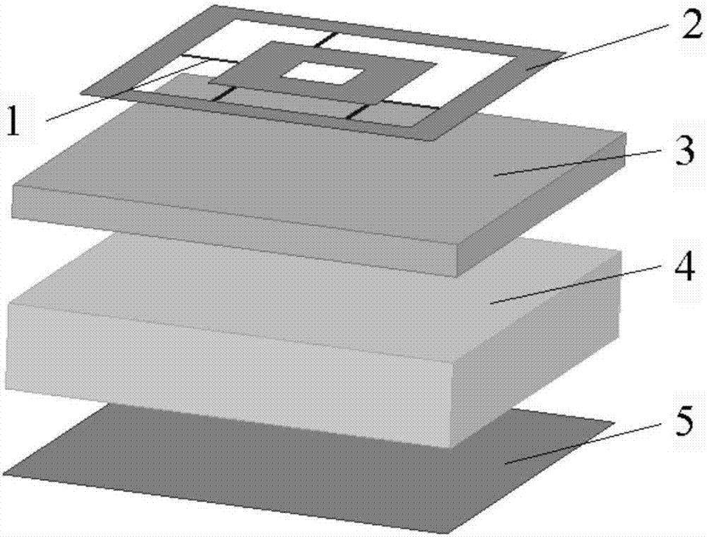
[0032] Such as figure 1 As shown, a schematic diagram of an electrically scanning planar reflectarray antenna unit based on a radio frequency switch, including a radio frequency switch 1 , an upper patch 2 , an upper dielectric 3 , a lower dielectric 4 and a ground plate 5 . Among them, 5 RF switches are used, and the unit is designed to work at 14GHz. The unit is a square with a side length equal to 0.5λ 0 ,λ 0 is the wavelength in free space. The thickness of the upper layer of the patch is 0.762mm, and the relative dielectric constant is 3.66; the thickness of the lower layer of the patch is 2mm, and the relative dielectric constant is 1.05; the bottom layer is the grounding plate.
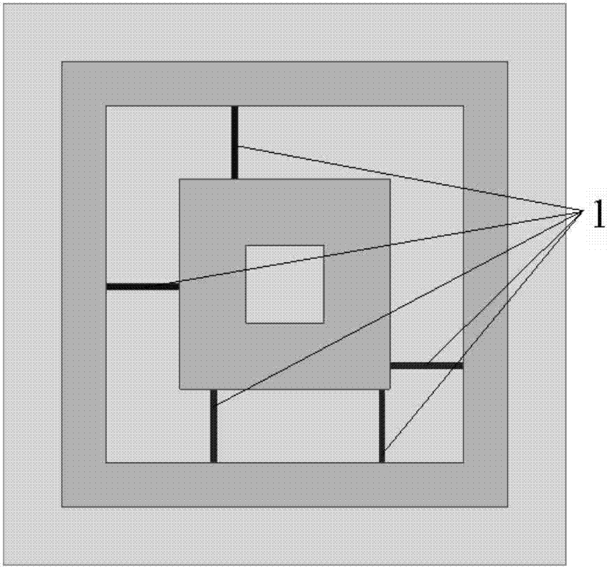
[0033] figure 2 A top view of the antenna unit is shown, 5 radio frequency switches are installed between two square rings of the upper patch 2, and the 5 switches are distributed at unequal intervals.
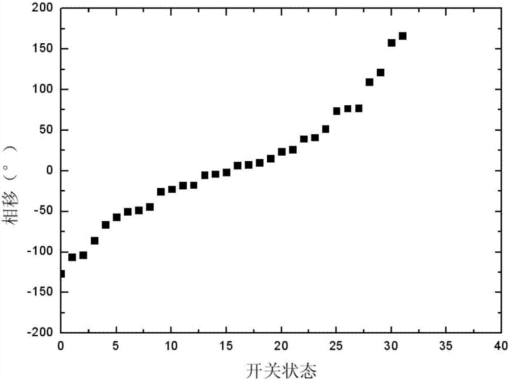
[0034] image 3 The graph shows the relationship between the switching state of the u...
PUM
| Property | Measurement | Unit |
|---|---|---|
| Media thickness | aaaaa | aaaaa |
| Media thickness | aaaaa | aaaaa |
Abstract
Description
Claims
Application Information


