Array substrate and detection method thereof and display device
An array substrate and substrate substrate technology, which is applied in optics, instruments, characters and pattern recognition, etc., can solve the problems of affecting the display effect of the display panel and the strong reflective performance of the metal light-shielding layer, and achieve the effect of reducing the impact and reducing the reflection.
- Summary
- Abstract
- Description
- Claims
- Application Information
AI Technical Summary
Problems solved by technology
Method used
Image

Examples
Embodiment Construction
[0037] Aiming at the problem in the prior art that the display effect of the display panel is affected due to the strong reflective performance of the metal light-shielding layer, an embodiment of the present invention provides an array substrate, a detection method thereof, and a display device.
[0038] The specific implementation manners of the array substrate provided by the embodiments of the present invention, its detection method and the display device will be described in detail below with reference to the accompanying drawings. The thickness and shape of each film layer in the drawings do not reflect the real scale, and the purpose is only to illustrate the content of the present invention.
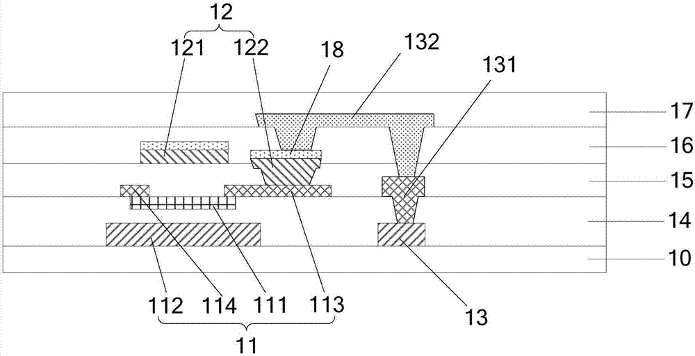
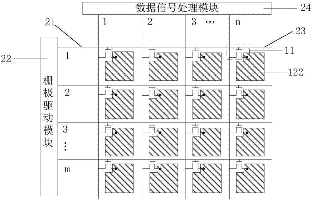
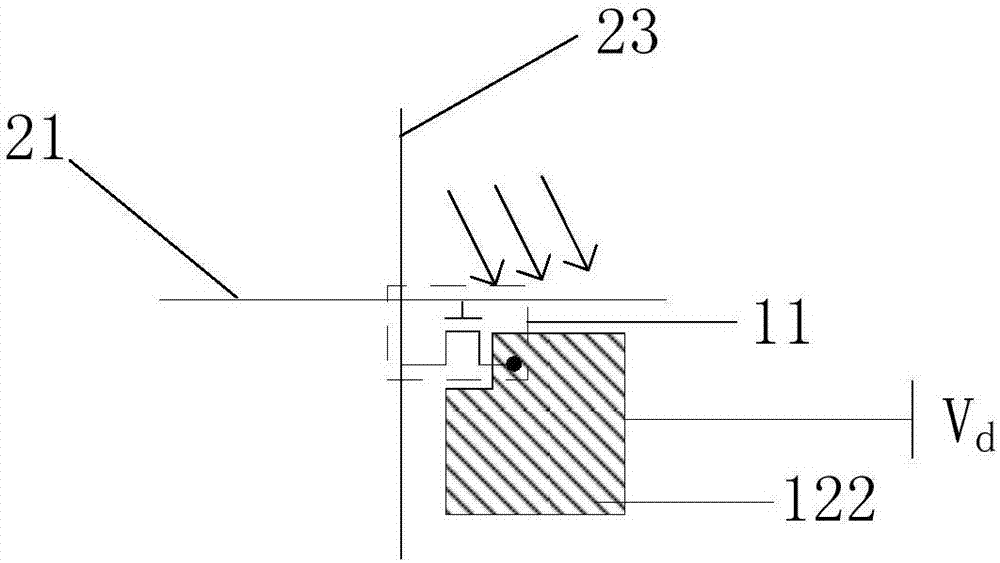
[0039] An embodiment of the present invention provides an array substrate, such as figure 1 As shown, it includes: a base substrate 10, a thin film transistor 11 located on the base substrate 10, such as a plurality of thin film transistors arranged in an array, and a photosensit...
PUM
 Abstract
Description
Claims
Application Information