Array substrate, preparation method thereof and display panel

An array substrate and display panel technology, which is applied in semiconductor/solid-state device manufacturing, instruments, semiconductor devices, etc., can solve the problems of lower contrast ratio of display panel, high reflectivity of display panel, and lower display effect of display panel, etc., so as to improve the display effect , Weaken the reflection and reduce the effect of reflectivity

Pending Publication Date: 2022-05-31
WUHAN CHINA STAR OPTOELECTRONICS TECH CO LTD
View PDF0 Cites 0 Cited by
  • Summary
  • Abstract
  • Description
  • Claims
  • Application Information

AI Technical Summary

Problems solved by technology

[0005] The purpose of the present invention is to provide an array substrate and its preparation method, and a display panel, which can solve the problem that there are many contact surfaces with large differences in refractive index in the exist

Method used


Image

  • Array substrate, preparation method thereof and display panel
  • Array substrate, preparation method thereof and display panel
  • Array substrate, preparation method thereof and display panel

Examples


Embodiment 1

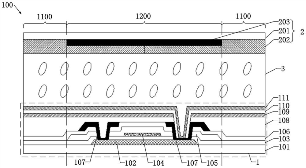
[0039] Such as figure 1 As shown, this embodiment provides a display panel 100 . The display panel 100 includes: an array substrate 1 , a color filter substrate 2 and a liquid crystal layer 3 .

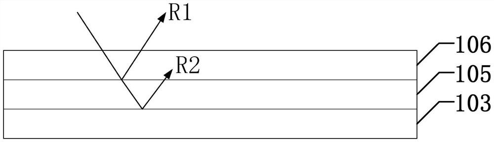
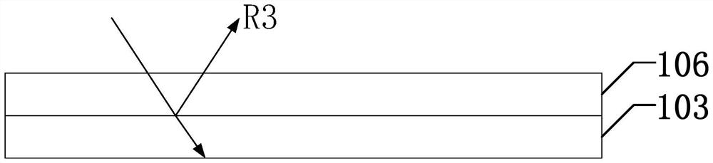
[0040] Wherein, the array substrate 1 includes an opening area 1100 and a non-opening area 1200 . The array substrate 1 includes: a first substrate 101, an active layer 102, a gate insulating layer 103, a gate layer 104, a first interlayer insulating layer 105, a second interlayer insulating layer 106, a source-drain layer 107, a flat layer 108 , a common electrode layer 109 , a passivation layer 110 and a pixel electrode layer 111 .

[0041]Wherein, the material of the first substrate 101 is one or more of glass, polyimide, polycarbonate, polyethylene terephthalate and polyethylene naphthalate, thus the first The substrate 101 can have better impact resistance and can effectively protect the display device 100 . In this embodiment, the material of the first substrate 101 is glass...


PUM


Abstract

The invention relates to an array substrate, a preparation method thereof and a display panel. The projection of a first interlayer insulating layer of the display panel on a first substrate is tangent to or separated from the projection of an opening area on the first substrate; the surface of the side, close to the first substrate, of the second interlayer insulating layer in the opening area is attached to the surface of the side, away from the first substrate, of the gate insulating layer, and the gate insulating layer and the second interlayer insulating layer are prepared through the same material. Therefore, the reflectivity of light rays on the contact surface of the second interlayer insulating layer and the gate insulating layer in the opening area can be reduced, the reflectivity of the display panel is further reduced, the reflection of the display panel to ambient light rays is weakened, the contrast ratio of the display panel is improved, and the display effect of the display panel is improved.

Description

technical field [0001] The present application relates to the field of display technology, in particular to an array substrate, a manufacturing method thereof, and a display panel. Background technique [0002] With the continuous popularization of electronic products, its innovation speed is very fast, and its functional requirements are becoming more and more stringent. Among them, the pursuit of lower reflectivity of display panels has also become the development trend of the future market. Lower reflectivity can bring users a more comfortable visual experience, especially in environments with strong external ambient light. [0003] After natural light enters the display panel, there are three main paths: transmission, absorption and reflection. Ideally, we hope that light can be completely transmitted or absorbed, but in reality, it is impossible to completely transmit or be absorbed by light. The main reason is that there are many film layers in the display panel, and...

Claims


Application Information

Patent Timeline
IPC IPC(8): H01L27/12H01L21/77G02F1/1362
CPCH01L27/1248H01L27/1222H01L27/1259G02F1/136209
Inventor 尹文
Owner WUHAN CHINA STAR OPTOELECTRONICS TECH CO LTD
Why Eureka
Try Eureka