
Near infrared absorber based on graphene/metal nanometer belt structure

A metal nano, graphene technology, applied in nano technology, nano optics, nano technology, etc., can solve problems such as difficulty, unsatisfactory absorption rate, and inability to achieve perfect absorption.

Inactive Publication Date: 2017-12-05
UNIV OF ELECTRONICS SCI & TECH OF CHINA
View PDF2 Cites 17 Cited by
  • Summary
  • Abstract
  • Description
  • Claims
  • Application Information

AI Technical Summary

Problems solved by technology

[0005] Under the guidance of this design concept, in 2014, Zhao et al. introduced graphene into the periodic silver nano-grating structure, and used the high-aspect-ratio silver grating to excite magneton resonance (MP) and the resistance effect of graphene to Improve the absorption rate of graphene to achieve perfect absorption, but because this kind of deep grating is difficult to process, it is not conducive to practical application
In 2015, the team of Xiamen University also introduced graphene into the absorber structure, combined with gold nanoribbons to stimulate the local surface plasmon effect, and realized the absorption of visible light band, but the absorption rate is not ideal
The results show that at a specific wavelength, graphene's absorption of electromagnetic waves increases by 16 times, but the absorption rate of the overall structure is only 60%, which still cannot achieve perfect absorption of specific wavelengths.

Method used


Image

  • Near infrared absorber based on graphene/metal nanometer belt structure
  • Near infrared absorber based on graphene/metal nanometer belt structure
  • Near infrared absorber based on graphene/metal nanometer belt structure

Examples


Embodiment Construction

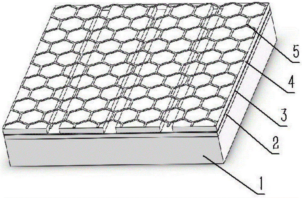
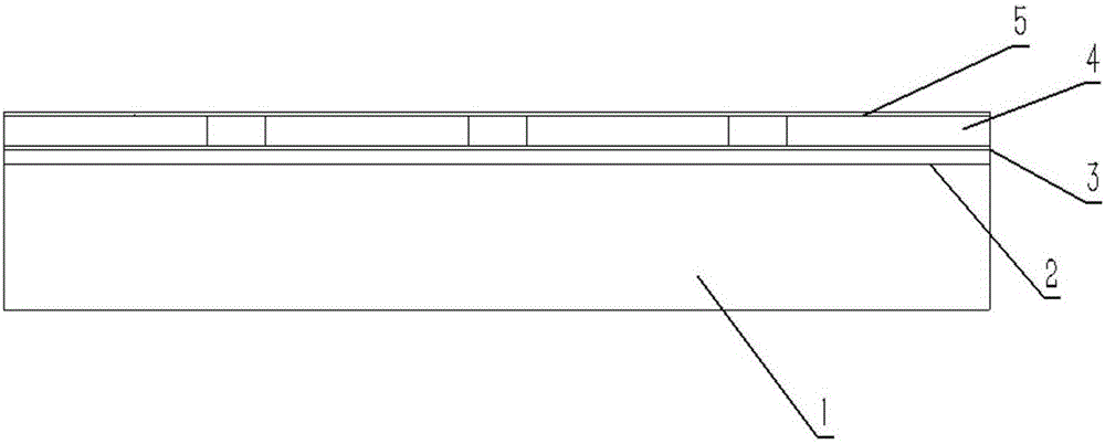
[0023] Such as figure 1 Shown, a kind of near-infrared absorber based on graphene / metal nanobelt structure is characterized in that it comprises substrate, graphene, metal nanobelt. The substrate includes (1) a silver substrate, (2) an oxide insulating layer, and the graphene layer includes (I) a first graphene layer, (II) a second graphene layer, wherein the first graphene layer is directly on the insulating layer 1. Under the metal nanobelt, the second graphene layer is arranged on the metal nanobelt.

[0024] The bottom layer of the substrate is silver, which reflects electromagnetic waves and is localized in the upper structure to prevent electromagnetic waves from being transmitted, with a thickness of 100nm.

[0025] The insulating layer is located on the base, and the dielectric material with low loss in the near-infrared band is selected: Al2O3, and the designed thickness is 5-15nm.

[0026] The first graphene layer is deposited on the insulating layer and is single...


PUM


Abstract

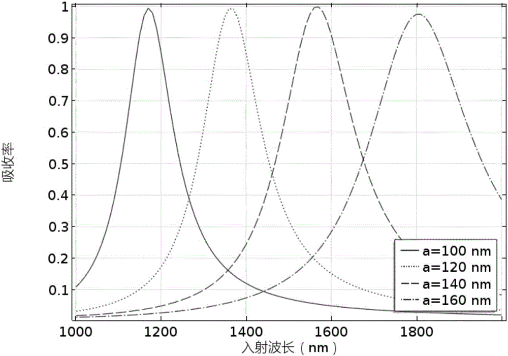
The invention relates to a near infrared absorber based on a graphene/metal nanometer belt structure and belongs to a perfect electromagnetic wave absorber. When incoming wave irradiates a metal nanometer belt array, the magnetic resonance effect is excited by the incoming wave at the metal nanometer belt, energy of the incoming wave is substantially enhanced at a gap of the metal nanometer belt, after upper and lower portions of the metal nanometer belt are respectively added with a graphene layer, electromagnetic wave energy is enhanced, the upper and lower graphene layer effect is enhanced, absorption is further carried out, and the resonance wavelength electromagnetic wave energy is integrally absorbed in a perfect mode. The near infrared absorber is advantaged in that five structure layers are comprised, sequentially comprising a substrate (1), an insulation layer (2), the first graphene layer (3), the metal nanometer belt (4) and the second graphene layer (5), and the specific wavelength can be absorbed to a nearly perfect degree through adjusting structural geometric parameters.

Description

technical field [0001] The invention belongs to the field of optoelectronic technology, and in particular relates to a structure design of a near-infrared absorber based on a graphene / metal nanobelt structure, which realizes near-perfect absorption of electromagnetic waves in the near-infrared band. Background technique [0002] In many fields such as photoelectric detection, solar energy, thermal sensing, and stealth technology, there are high requirements for the absorption performance of photoelectric materials, and a high absorption rate for electromagnetic wave energy is required. Optoelectronic devices such as photoelectric detection and photovoltaic devices rely on photoelectric materials to convert absorbed light into electrical energy or electrical signals to achieve their functions. Under a certain conversion efficiency, the more light absorbed, the stronger the electrical signal generated. The larger it is, the higher the efficiency of the optoelectronic device as...

Claims


Application Information

Patent Timeline
Patent Type & Authority Applications(China)
IPC IPC(8): G01J1/42B82Y20/00
CPCG01J1/42B82Y20/00
Inventor 张晓霞陈浩姬月华余力皮峣迪
Owner UNIV OF ELECTRONICS SCI & TECH OF CHINA
Learn More