Pixel circuit, driving method of pixel circuit, display panel and display device

A technology for pixel circuits and driving transistors, applied in the fields of pixel circuits, display panels and display devices, can solve problems such as image sticking, threshold voltage shift, etc., and achieve the effect of restoring threshold voltage shift and avoiding sticking phenomenon.

Active Publication Date: 2017-12-08
WUHAN TIANMA MICRO ELECTRONICS CO LTD
View PDF6 Cites 14 Cited by
  • Summary
  • Abstract
  • Description
  • Claims
  • Application Information

AI Technical Summary

Problems solved by technology

[0004] Embodiments of the present invention provide a pixel circuit, a driving method thereof, a display panel, and a display device, which are used to improve the problem of image sticking caused by the threshold voltage shift of the driving transistor caused by long-term bias voltage in the existing pixel circuit

Method used


Image

  • Pixel circuit, driving method of pixel circuit, display panel and display device
  • Pixel circuit, driving method of pixel circuit, display panel and display device
  • Pixel circuit, driving method of pixel circuit, display panel and display device

Examples


example 1

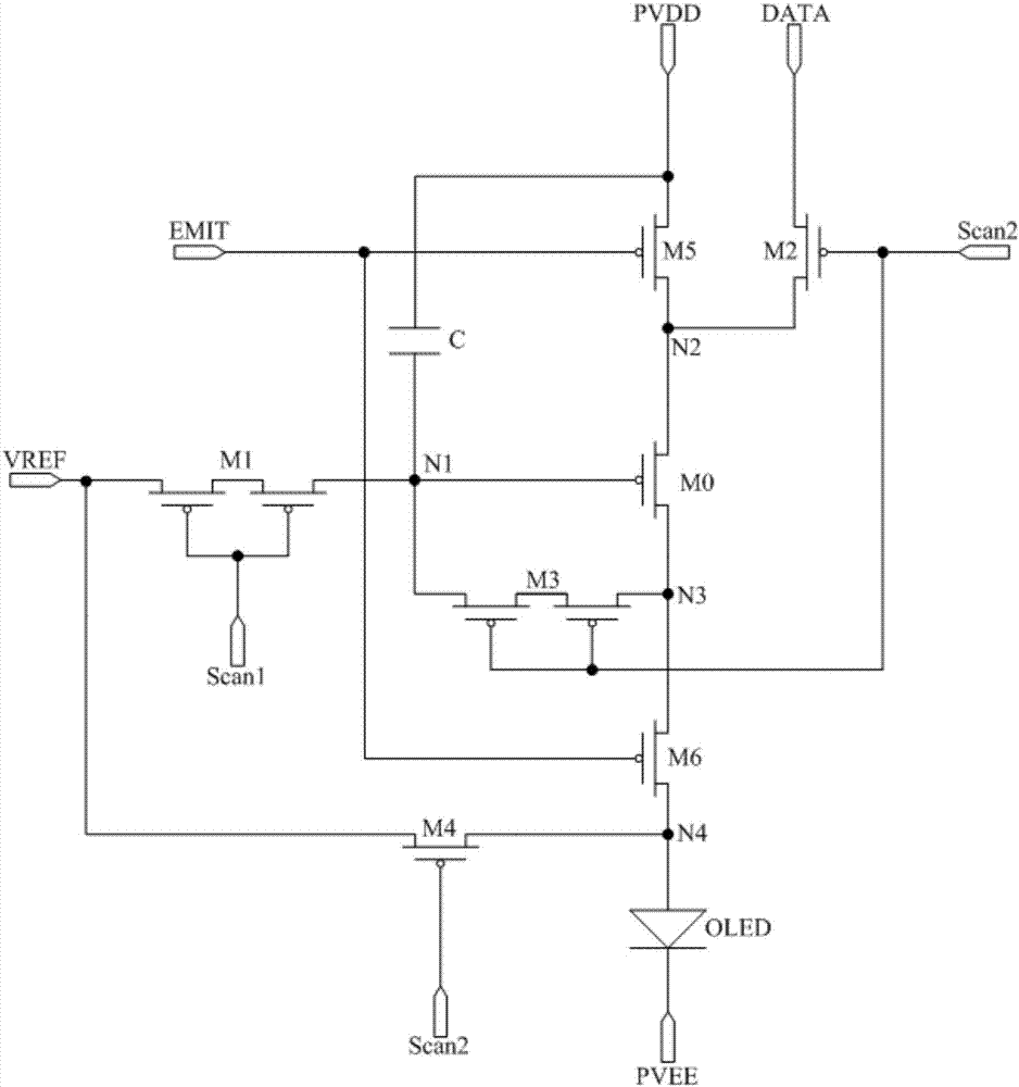
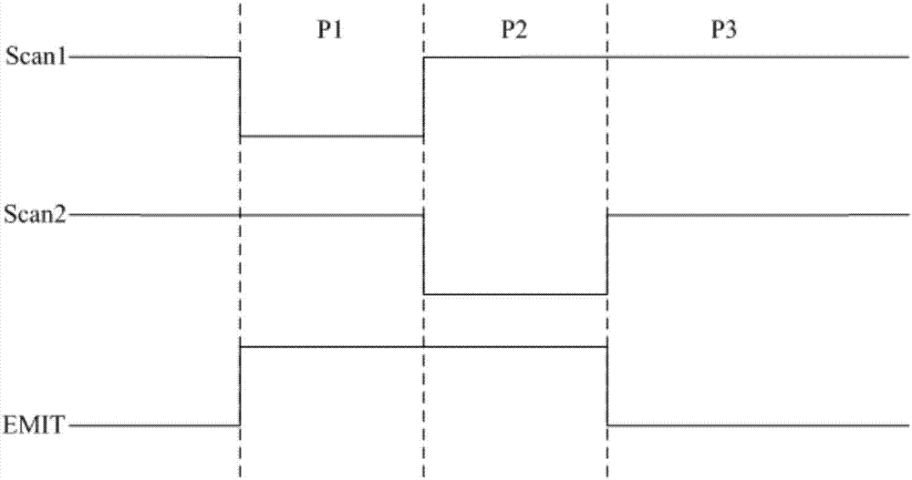
[0075] by Figure 4 Take the pixel circuit shown as an example, and the corresponding input and output timings are as follows Figure 8a shown. Specifically, choose the Figure 8a The three stages of T1, T2, and T3 in the input timing diagram shown.

[0076] In node initialization phase T1, Scan1=0, Scan2=1, Scan3=0, EMIT1=1, EMIT2=0.

[0077] Since Scan1=0, the first switching transistor M1 is turned on to provide the reference signal of the reference signal terminal VREF to the gate of the driving transistor M0, and the potential of the gate of the driving transistor M0 is VREF. Since Scan3=0, the third switching transistor M3 is turned on to provide the reference signal received by the gate of the driving transistor M0 to the second pole of the driving transistor M0, the potential of the second pole of the driving transistor M0 is VREF, and the driving transistor M0 The gate of M0 and the second pole of the driving transistor M0 are initialized and reset. Since EMIT2=0...

example 2

[0086] by Figure 5 Take the pixel circuit shown as an example, and the corresponding input and output timings are as follows Figure 9a shown. Specifically, choose the Figure 9a The three stages of T1, T2, and T3 in the input timing diagram shown.

[0087] In node initialization phase T1, Scan1=0, Scan2=1, EMIT1=1, EMIT2=0.

[0088] Since Scan1=0, the first switching transistor M1 is turned on to provide the reference signal of the reference signal terminal VREF to the gate of the driving transistor M0, and the potential of the gate of the driving transistor M0 is VREF. Since EMIT1=1, the third switching transistor M3 is turned on to provide the reference signal received by the gate of the driving transistor M0 to the second pole of the driving transistor M0, the potential of the second pole of the driving transistor M0 is VREF, and the driving transistor M0 The gate of M0 and the second pole of the driving transistor M0 are initialized and reset. Since EMIT2=0, the fif...

example 3

[0097] by Image 6 Take the pixel circuit shown as an example, and the corresponding input and output timings are as follows Figure 10a shown. Specifically, choose the Figure 10a The three stages of T1, T2, and T3 in the input timing diagram shown.

[0098] In node initialization phase T1, Scan1=1, Scan2=0, EMIT1=0, EMIT2=1.

[0099] Since Scan1=1, the first switching transistor M1 is turned on to provide the reference signal of the reference signal terminal VREF to the gate of the driving transistor M0, and the potential of the gate of the driving transistor M0 is VREF. Since EMIT1=0, the third switching transistor M3 is turned on to provide the reference signal received by the gate of the driving transistor M0 to the second pole of the driving transistor M0, the potential of the second pole of the driving transistor M0 is VREF, and the driving transistor M0 The gate of M0 and the second pole of the driving transistor M0 are initialized and reset. Since EMIT2=1, the fi...


PUM


Abstract

The invention discloses a pixel circuit, a driving method of the pixel circuit, a display panel and a display device. The pixel circuit comprises a node initialization module, a data writing module, a coupling module, a luminescence control module, a drive transistor and a luminescent component, wherein before luminescence of the luminescent component, the node initialization module provides a reference signal to a grid of the drive transistor; and the data writing module is used for conducting a third switching transistor when the reference signal is written into the grid of the drive transistor by virtue of the node initialization module, so that the reference signal, which is received by the grid of the drive transistor, is driven to be provided to a second electrode of the drive transistor. By simultaneously resetting the grid and the second electrode of the drive transistor in an initialization stage, current directions in the initialization stage and in a data writing stage can be kept opposite to a current direction in a luminescence stage, threshold voltage deviation, caused by long-time bias, of the drive transistor can be recovered, and subsequently, the occurrence of a ghosting phenomenon can be prevented.

Description

technical field [0001] The present invention relates to the field of display technology, in particular to a pixel circuit, a driving method thereof, a display panel and a display device. Background technique [0002] Organic Light Emitting Diode (OLED) is one of the hot spots in the field of flat panel display research today. Compared with liquid crystal displays, OLED has the advantages of low energy consumption, low production cost, self-illumination, wide viewing angle and fast response speed. , OLEDs have begun to replace traditional Liquid Crystal Displays (LCDs) in the field of flat panel displays such as mobile phones, PDAs, and digital cameras. Among them, pixel circuit design is the core technical content of OLED display, which has important research significance. [0003] The structure of an existing pixel circuit is as follows figure 1 as shown, figure 1 It is a structure diagram of an existing pixel circuit, including 6 switching transistors: M1-M6, 1 driving ...

Claims


Application Information

Patent Timeline
Patent Type & Authority Applications(China)
IPC IPC(8): G09G3/3225
CPCG09G3/3225G09G2320/0257
Inventor 高娅娜朱仁远李玥向东旭陈泽源蔡中兰
Owner WUHAN TIANMA MICRO ELECTRONICS CO LTD
Why Eureka
Try Eureka