
Chip fan-out packaging structure, multi-chip integrated module and wafer-level packaging method

A packaging structure and chip technology, which is applied in the direction of antenna support/mounting device, circuit, electric solid device, etc., can solve the problems of difficult ground connection of conductive layer, continuity of difficult conductive layer, rough surface, etc., and achieves low cost and low production cost The effect of cost reduction and simple production process

Active Publication Date: 2020-04-17
HUATIAN TECH KUNSHAN ELECTRONICS
View PDF3 Cites 0 Cited by
  • Summary
  • Abstract
  • Description
  • Claims
  • Application Information

AI Technical Summary

Problems solved by technology

Because it is a chip-level process, it is time-consuming; and the surface after packaging is rough, it is difficult to ensure the continuity of the conductive layer, and it is also difficult to make the ground connection of the conductive layer

Method used


Image

  • Chip fan-out packaging structure, multi-chip integrated module and wafer-level packaging method
  • Chip fan-out packaging structure, multi-chip integrated module and wafer-level packaging method
  • Chip fan-out packaging structure, multi-chip integrated module and wafer-level packaging method

Examples


Embodiment Construction

[0041] In order to understand the technical content of the present invention more clearly, the following examples are given in detail, the purpose of which is only to better understand the content of the present invention but not to limit the protection scope of the present invention. The components in the structures in the drawings of the embodiments are not scaled according to the normal scale, so they do not represent the actual relative sizes of the structures in the embodiments.

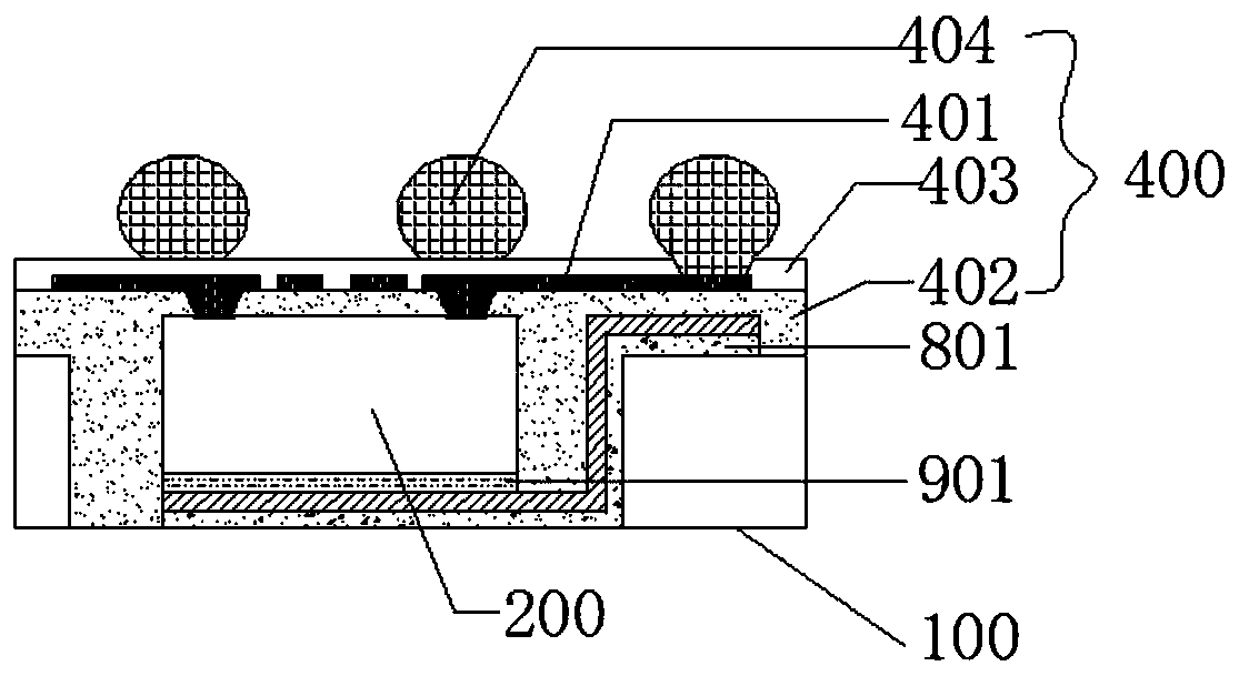
[0042] Such as figure 1 As shown, a chip fan-out packaging structure with an integrated antenna includes a carrier board 100 and at least one radio frequency chip 200 including a radio frequency signal receiving or / and transmitting function, and the carrier board has a first surface and a second surface opposite to it. On the surface, the carrier board has a first groove 101 for accommodating the radio frequency chip, and the bonding pad of the radio frequency chip is buried in the first groove ...


PUM


Abstract

The invention discloses a chip fan-out packaging structure having an antenna, a multichip integrated module and a wafer level packaging method. The antenna is formed in the first groove of a support plate used for accommodating a radio frequency chip and extends to the first surface of the support plate, and then a first metal rewiring layer is formed on the radio frequency chip and the first surface of the support plate so that interconnection between the antenna and the chip can be realized, the function of chip level antenna integration can be achieved without occupying the area of the metal interconnection layer in the chip, and the manufacturing cost can be greatly reduced. According to the multichip integrated module, electromagnetic interference shielding of the functional chip and antenna integration of the radio frequency chip can be simultaneously realized so that the production technology is simple without time consumption, the cost is low without the problems that the surface of the packaging body is rough after packaging and the continuity of the electromagnetic interference shielding structure is difficult to guarantee, and grounding connection can be more easily manufactured in comparison with the conventional method. According to the wafer level packaging method, the method is low in cost and high in efficiency, and the electromagnetic interference shielding structure and the antenna are simultaneously integrated so that the manufacturing cost can be greatly reduced.

Description

technical field [0001] The invention relates to the technical field of fan-out wafer-level packaging, in particular to a chip fan-out packaging structure for an integrated antenna, a multi-chip integrated module and a wafer-level packaging method. Background technique [0002] Fan-out wafer-level packaging is to realize fan-out packaging of chips at the wafer size level. It is also an advanced packaging process with a large number of I / Os and good integration flexibility. It can realize vertical and horizontal multi-chip integration in one package. . As such, fan-out wafer-level packaging is currently being developed into next-generation packaging technologies such as multi-die, low-profile packaging, and 3D SiP. With the development of electronic products in the direction of thinner, lighter, higher pin density, and lower cost, the emergence of fan-out wafer-level packaging technology provides an opportunity for the packaging industry to develop multi-functional small-size...

Claims


Application Information

Patent Timeline
Patent Type & Authority Patents(China)
IPC IPC(8): H01L23/66H01L23/552H01L25/16H01L21/98H01L23/488H01Q1/22
CPCH01L23/552H01L23/66H01L24/02H01L25/16H01L25/50H01L2223/6677H01L2224/023H01L2224/0231H01Q1/2283H01L2224/04105H01L2224/12105H01L2224/19H01L2224/24137H01L2224/32225H01L2224/32245H01L2224/73267H01L2224/92244H01L2924/15153H01L2924/3025
Inventor 王腾
Owner HUATIAN TECH KUNSHAN ELECTRONICS
Learn More