Flexible substrate and method for manufacturing the same, flexible display device and flexible display apparatus

A flexible substrate and manufacturing method technology, applied in the field of flexible display devices, can solve the problems of display device damage, difficulty in ensuring uniformity, huge investment, etc., and achieve the effect of ensuring tight fit and avoiding falling off

Inactive Publication Date: 2017-12-15
BOE TECH GRP CO LTD +1
View PDF3 Cites 9 Cited by
  • Summary
  • Abstract
  • Description
  • Claims
  • Application Information

AI Technical Summary

Problems solved by technology

Laser peeling requires the use of special laser equipment, which requires a huge investment, and takes a long time, and the uniformity is difficult to guaran

Method used


Image

  • Flexible substrate and method for manufacturing the same, flexible display device and flexible display apparatus
  • Flexible substrate and method for manufacturing the same, flexible display device and flexible display apparatus
  • Flexible substrate and method for manufacturing the same, flexible display device and flexible display apparatus

Examples


Example Embodiment

[0020] Example one

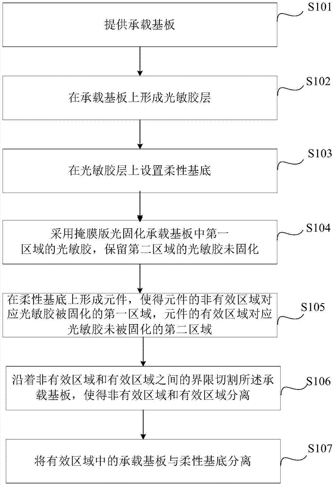
[0021] The embodiment of the present invention provides a method for manufacturing a flexible substrate, figure 1 It is a process flow chart of a method for manufacturing a flexible substrate according to an embodiment of the present invention.

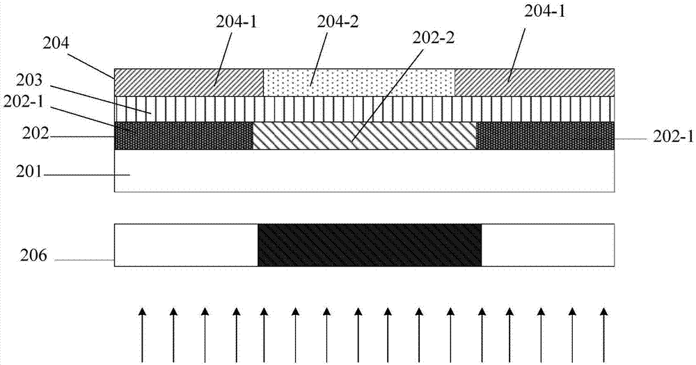
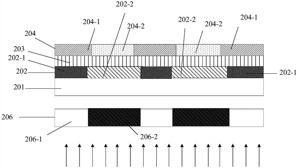
[0022] Such as figure 1 As shown, the method includes: first, in step S101, a carrier substrate 201 is provided; then in step S102, a photosensitive adhesive layer 202 is formed on the carrier substrate 201; then in step S103, a flexible adhesive layer 202 is provided on the photosensitive adhesive layer 202. 基基203。 Base 203. The method of setting the flexible substrate 203 can directly attach a flexible substrate film after the photosensitive adhesive layer is coated to form a flexible substrate; or apply a flexible liquid material on the photosensitive adhesive layer, and then solidify to form a flexible substrate, by coating a flexible liquid material Then, the thickness of the flexible substrate formed by the metho...

Example Embodiment

[0035] Example two

[0036] The embodiment of the present invention provides a flexible substrate manufactured using the method provided in the first embodiment, and also provides a flexible display device manufactured using the method provided in the first embodiment. The device is a display device, including a liquid crystal display and an organic light emitting device. A diode or electrophoretic display also provides a flexible display device, including the above-mentioned flexible display device.


PUM


Abstract

The invention provides a method for manufacturing a flexible substrate. The method includes that a bearing substrate is provided; a photosensitive adhesive layer is formed on the bearing substrate; a flexible substrate is arranged on the photosensitive adhesive layer, the flexible substrate includes an active area and an inactive area; the photosensitive adhesive layer comprises a first area and a second area, the photosensitive adhesive in the first area in the photosensitive adhesive layer is light-cured and the photosensitive adhesive in the second area remains uncured; a component is formed on the flexible substrate, the orthographic projection of the inactive area of the flexible substrate on the bearing substrate covers the orthographic projection of the first area of the photosensitive adhesive layer on the bearing substrate, the orthogonal projection of the second area of the photosensitive adhesive layer on the bearing substrate covers the orthogonal projection of the active area of the flexible substrate on the bearing substrate; the bearing substrate is cut along the boundary between the inactive area and the active area such that the inactive area and the active area are separated; and the bearing substrate in the active area is separated from the flexible substrate. The method can effectively reduce the peel strength between the flexible substrate and the bearing substrate.

Description

technical field [0001] The present invention relates to the technical field of display devices, in particular to a method for manufacturing a flexible substrate, a flexible substrate, a flexible display device and a flexible display device. Background technique [0002] At present, flexible display devices, including flexible organic light-emitting diodes (OLEDs), flexible liquid crystal displays (LCDs), and flexible electronic papers, are generally manufactured by coating or laminating flexible substrates on hard substrates (most typically glass substrates). Thin film substrate, after the display device is formed, the flexible film substrate with the display device is peeled off from the hard substrate. Polyimide (PI) is often used as a flexible film substrate in flexible display devices because it is a high-quality high-temperature-resistant flexible material. There are two methods for peeling polyimide flexible film substrates from hard substrates, one is laser peeling, ...

Claims


Application Information

Patent Timeline
IPC IPC(8): H01L27/12H01L21/683
CPCH01L21/6835H01L27/1218H01L2221/68345G02F1/133305Y02E10/549G02F1/133388Y02P70/50H10K77/111H10K2102/311H10K71/00
Inventor 张俊瑞
Owner BOE TECH GRP CO LTD
Why Eureka
Try Eureka