Semiconductor device and method for writing/reading information
一种半导体、读取部的技术,应用在信息存储、数字存储器信息、静态存储器等方向,能够解决消耗电力大、数据搜寻装置电路构成复杂、问题未提出根本的解决方案等问题
- Summary
- Abstract
- Description
- Claims
- Application Information
AI Technical Summary
Problems solved by technology
Method used
Image

Examples
Embodiment Construction
[0079] Hereinafter, modes for implementing the present invention will be described using icons. However, the present invention is not limited to the forms described below, but also includes forms that are appropriately modified from the following forms within the obvious range by those skilled in the art.
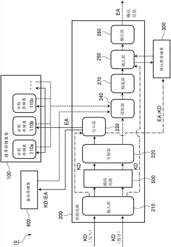
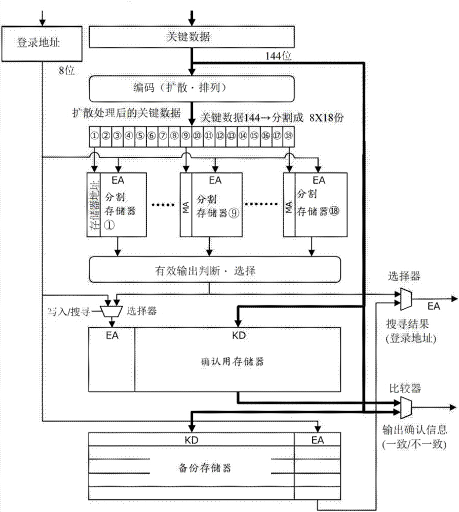
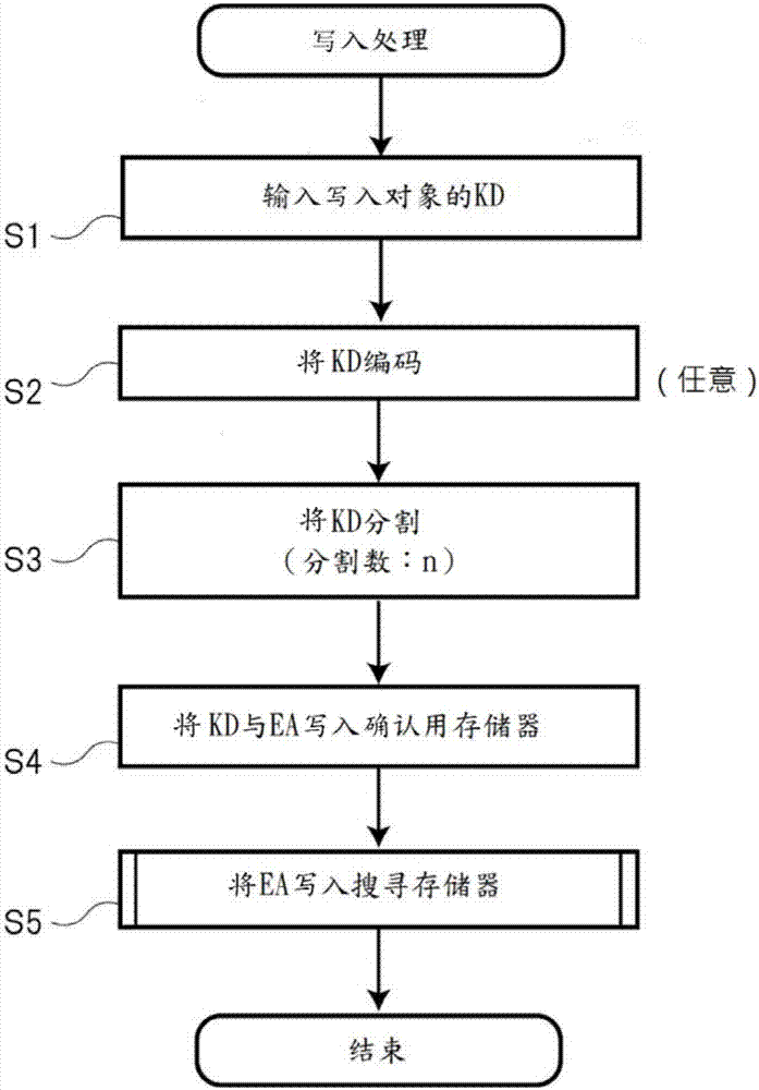
[0080] figure 1 is a functional block diagram showing the main functional configuration constituting the semiconductor device 10, and figure 2 It is a flowchart showing the processing flow of the semiconductor device 10 . further, Figure 3 ~ Figure 7 It is a diagram showing an example of the writing process of the registration address of the semiconductor device 10, Figure 8 ~ Figure 11 It is a diagram showing an example of reading processing (search processing) of the registered address of the semiconductor device 10 .
[0081] Such as figure 1 As shown, the semiconductor device 10 basically includes a search memory pad 100 , a control circuit 200 and a confirmatio...
PUM
 Abstract
Description
Claims
Application Information
 - Generate Ideas
- Intellectual Property
- Life Sciences
- Materials
- Tech Scout
- Unparalleled Data Quality
- Higher Quality Content
- 60% Fewer Hallucinations
Browse by: Latest US Patents, China's latest patents, Technical Efficacy Thesaurus, Application Domain, Technology Topic, Popular Technical Reports.
© 2025 PatSnap. All rights reserved.Legal|Privacy policy|Modern Slavery Act Transparency Statement|Sitemap|About US| Contact US: help@patsnap.com