
A kind of oled display backplane and preparation method thereof

A display backplane and bending area technology, which is applied in semiconductor/solid-state device manufacturing, semiconductor devices, electrical components, etc., can solve problems affecting the bending success rate and product yield of OLED display backplanes, and poor contact of circuits in the backplane , metal wire stress concentration and other problems, to achieve the effect of improving product mass production yield, improving bending success rate, and reducing stress concentration

Active Publication Date: 2021-04-13
BOE TECH GRP CO LTD +1
View PDF1 Cites 0 Cited by
  • Summary
  • Abstract
  • Description
  • Claims
  • Application Information

AI Technical Summary

Problems solved by technology

[0003] At present, when the bending process is performed on the bending area of ​​the OLED display backplane, because the bending area generates a large stress during bending, and it is easy to form sharp corners or asymmetrical bending in the bending area after bending, resulting in The stress concentration of the metal wires located in the bending area will cause the metal wires to break, resulting in poor contact of the circuit in the backplane, affecting the success rate of bending and product yield of the OLED display backplane

Method used


Image

  • A kind of oled display backplane and preparation method thereof
  • A kind of oled display backplane and preparation method thereof
  • A kind of oled display backplane and preparation method thereof

Examples


Embodiment Construction

[0032] The following will clearly and completely describe the technical solutions in the embodiments of the present invention with reference to the accompanying drawings in the embodiments of the present invention. Obviously, the described embodiments are only some, not all, embodiments of the present invention. Based on the embodiments of the present invention, all other embodiments obtained by persons of ordinary skill in the art without making creative efforts belong to the protection scope of the present invention.

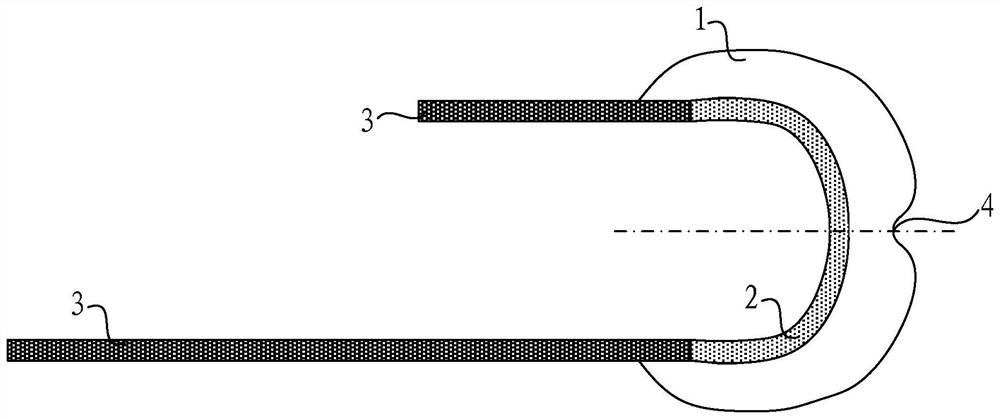
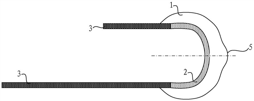
[0033] Such as figure 1 , figure 2 , image 3 as well as Figure 4 As shown, an OLED display backplane includes a bending area 2 and a non-bending area 3, the surface of the bending area 2 has an adhesive layer 1, and the adhesive layer 1 forms a buffer structure for buffering the bending stress of the bending area 2 , the cushioning structure is located at the central axis of the bending zone 2 , and the central axis of the cushioning structure coincides ...


PUM


Abstract

The invention relates to the field of display technology, and discloses an OLED display backplane and a preparation method thereof. The OLED display backplane includes a bending area and a non-bending area, and the surface of the bending area has an adhesive layer, which is formed to buffer the bend. The buffer structure of the bending stress in the bending area. The buffer structure is located at the central axis of the bending area, and the central axis of the buffering structure coincides with the central axis of the bending area. The bending area generates a large stress when it is bent. Buffer structure, and through the buffering effect of the buffer structure, the phenomenon of stress concentration of the metal wire in the bending area is avoided, which in turn can reduce the breakage of the internal metal wire when bending in the bending area, and improve the success rate of bending; the bending area Symmetrical bending can be achieved relatively easily during bending, and the bending operation can be realized more conveniently, which improves the success rate of bending, reduces the stress concentration phenomenon in the bending area, and makes it easier to form symmetrical bending, which in turn is beneficial Improve the success rate of OLED display backplane bending, and improve the mass production yield of products.

Description

technical field [0001] The invention relates to the field of display technology, in particular to an OLED display backplane and a preparation method thereof. Background technique [0002] With the advancement of display technology, the screens of electronic display products are becoming more and more narrow frame or even frameless, especially for OLED (Organic Light Emitting Diode) display devices. At present, flexible backplane bending is an important way to reduce the lower frame of display devices. Technical means, the narrowing of the lower frame of the OLED display backplane is mainly realized by bending the OLED display backplane. [0003] At present, when the bending process is carried out on the bending area of ​​the OLED display backplane, because the bending area generates large stress during bending, and it is easy to form sharp corners or asymmetrical bending in the bending area after bending, resulting in The stress concentration of the metal wires located in t...

Claims


Application Information

Patent Timeline
Patent Type & Authority Patents(China)
IPC IPC(8): H01L51/00H01L51/56H10K99/00
CPCH10K77/111H10K59/8722H10K71/00H10K50/8426H10K50/844H10K59/40
Inventor 王研鑫王松杨恕权黄鹏
Owner BOE TECH GRP CO LTD
Learn More