Single-ended negative feedback charge pump for delay-locked loop
A delay-locked loop, charge pump technology, applied in the direction of electrical components, power automatic control, etc., can solve the problems of Vctrl change, unable to suppress the current source mismatch well, to suppress the current mismatch problem, weaken the time dithering effect
- Summary
- Abstract
- Description
- Claims
- Application Information
AI Technical Summary
Problems solved by technology
Method used
Image
Examples
Embodiment Construction
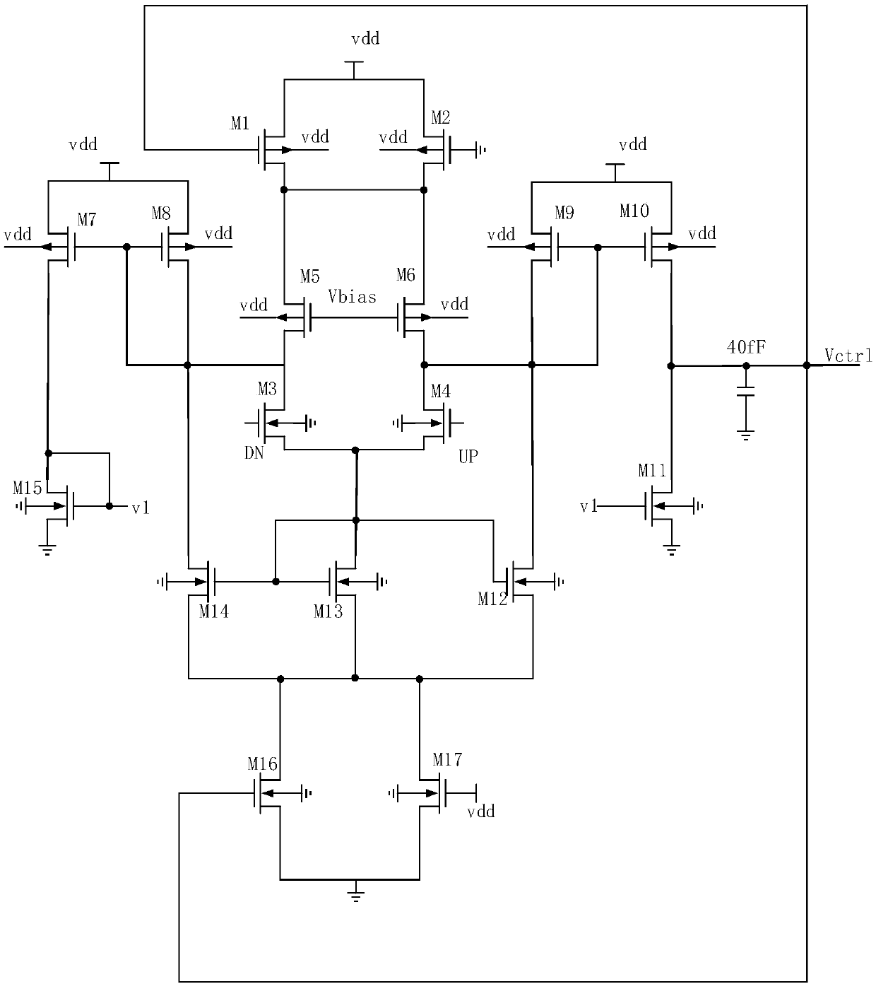
[0014] The new charge pump structure proposed by the present invention is as Figure three As shown: the sources of the two PMOS transistors M1 and M2 are connected to the drain of the power supply vdd, the gate of M2 is grounded, and the gate of M1 is connected to the final output Vctrl. The sources of PMOS transistors M5 and M6 are connected to the drain of M1, and the gates are connected. The gate voltage Vbias is 0.8V. The drains of M5 and M6 are respectively connected to the drains of NMOS transistors M3 and M4, and the gates of M3 and M4 are respectively input The DN and UP signals are connected to the source and connected to the gates of NMOS transistors M12, M13 and M14, where the gate and drain of M13 are connected, the drains of M14 and M12 are respectively connected to the drains of M3 and M4, and the gates of M12, M13 and M14 The sources are connected and connected to the drains of NMOS transistors M16 and M17, the gate of M17 is connected to the power supply vdd, ...
PUM
 Abstract
Description
Claims
Application Information


