Making method of OLED panel and OLED panel

A manufacturing method and panel technology, which are applied in the manufacture of OLED panels and in the field of OLED panels, can solve the problem of uneven display of OLED panels, and achieve the effect of improving uneven display.

Pending Publication Date: 2018-01-19
SHENZHEN CHINA STAR OPTOELECTRONICS SEMICON DISPLAY TECH CO LTD
View PDF8 Cites 28 Cited by
  • Summary
  • Abstract
  • Description
  • Claims
  • Application Information

AI Technical Summary

Problems solved by technology

[0006] The object of the present invention is to provide a method for manufacturing an OLED panel. The prepared OLED panel has an auxiliary electrode connected to the cathode, which can improve the problem of uneven display of the OLED panel caused by the IR voltage drop of the cathode.

Method used


Image

  • Making method of OLED panel and OLED panel
  • Making method of OLED panel and OLED panel
  • Making method of OLED panel and OLED panel

Examples


Embodiment Construction

[0057] In order to further illustrate the technical means adopted by the present invention and its effects, the following describes in detail in conjunction with preferred embodiments of the present invention and accompanying drawings.

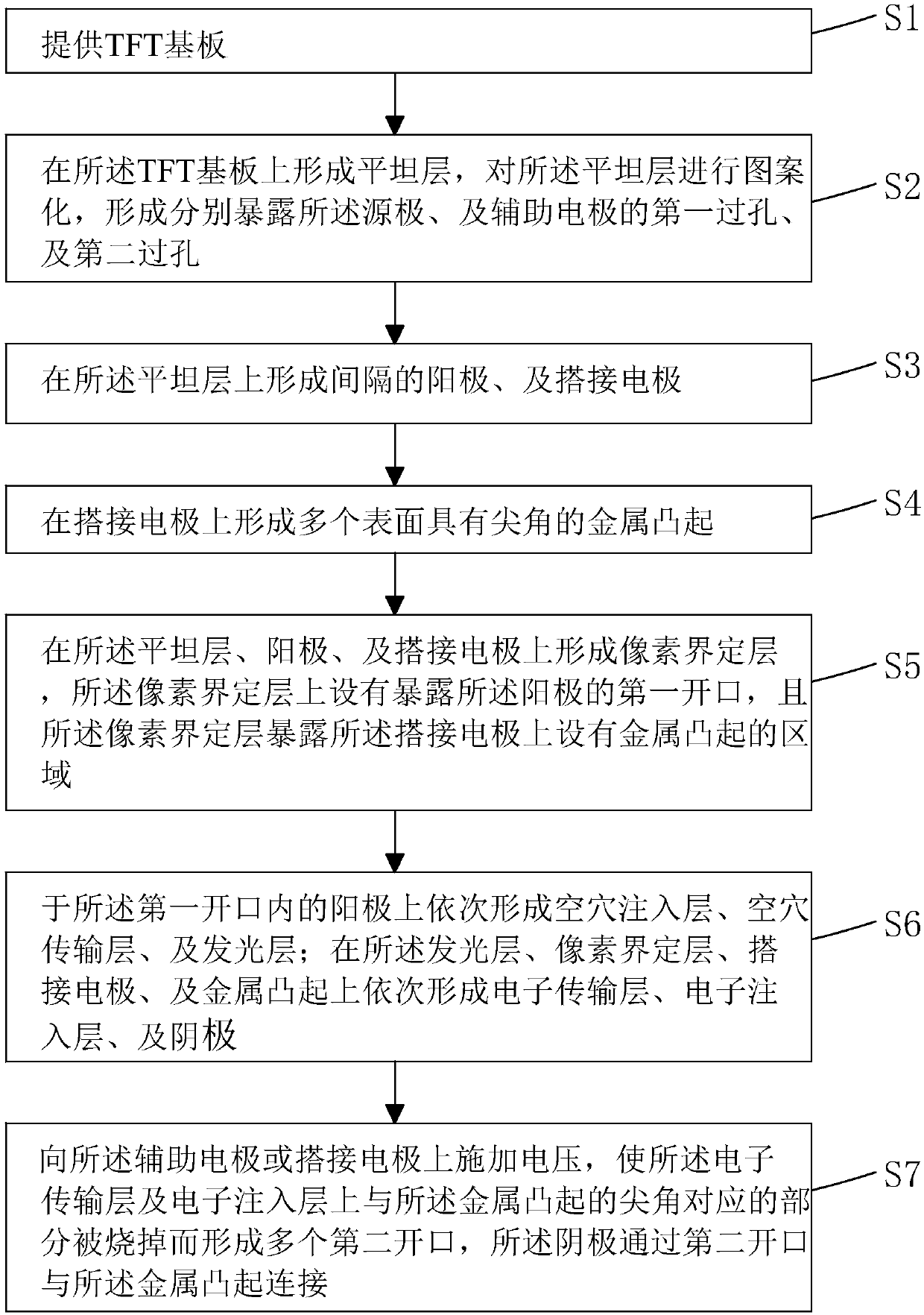
[0058] see figure 1 , the invention provides a method for manufacturing an OLED panel, comprising the steps of:

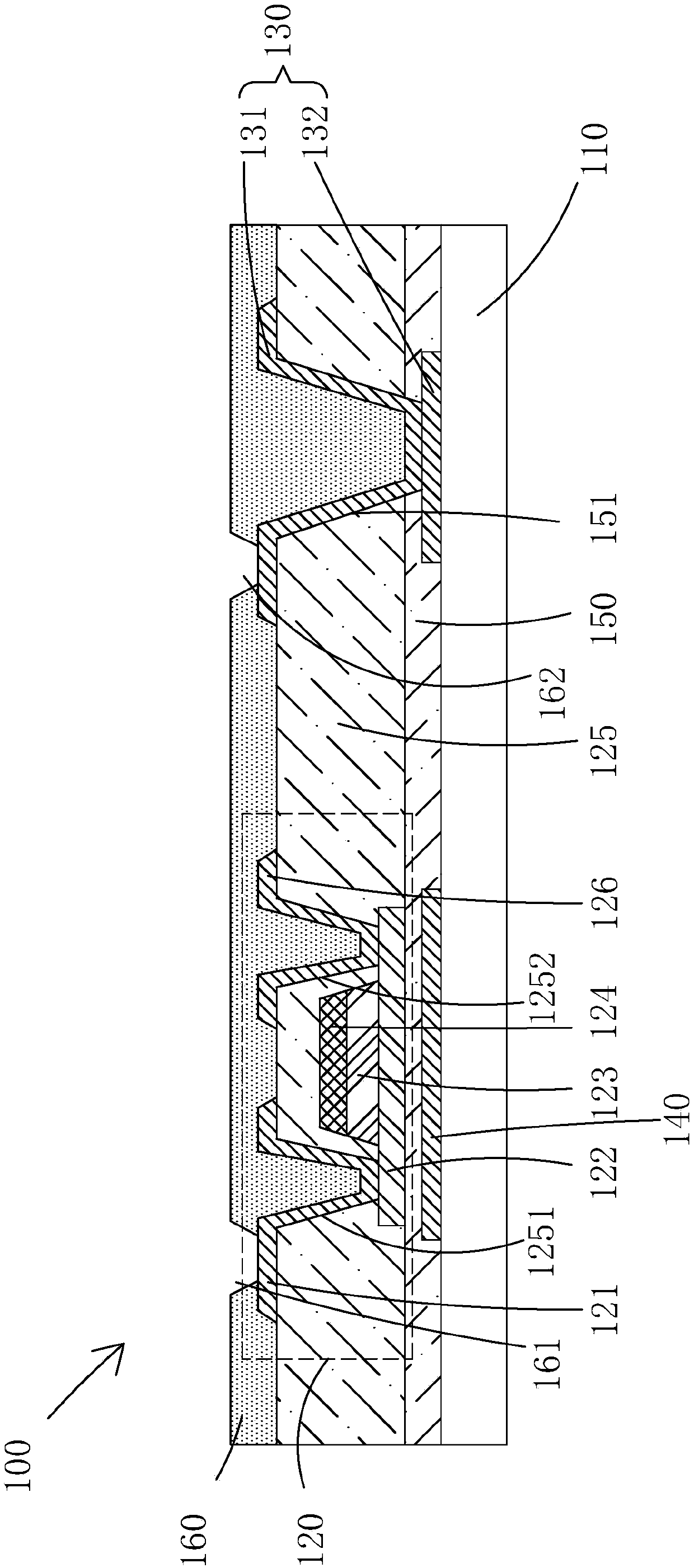
[0059] Step S1, please refer to figure 2 , providing a TFT substrate 100;

[0060] The TFT substrate 100 includes: a base substrate 110 , and a TFT 120 and an auxiliary electrode 130 disposed on the base substrate 110 and separated from each other; the TFT 120 has a source 121 .

[0061] Specifically, in figure 2 In the illustrated embodiment, the TFT 120 is a top gate thin film transistor, comprising: an active layer 122 disposed above the base substrate 110, and sequentially disposed on the active layer 122 The gate insulating layer 123 and the gate 124, the interlayer insulating layer 125 covering the active layer 122 and ...


PUM


Abstract

The invention provides a making method of an OLED panel and an OLED panel, wherein the making method of the OLED panel is characterized by making an anode connected with a source cathode of a TFT anda lapping electrode connected with an auxiliary electrode on a TFT substrate; making a plurality of metal salients with cusps on the surfaces in the lapping electrode; after successively forming an electrical transmission layer, an electrical injection layer and a cathode with whole surfaces in the subsequent making process, the positions of the electrical transmission layer and the electrical injection layer corresponding to the cusps of the metal salients are provided with slim film thicknesses; after further applying voltage to the auxiliary electrode and the lapping electrode, the positions of the electrical transmission layer and the electrical injection layer corresponding to the cusps of the metal salients are burnt by the cusps of the metal salients because of big impedance; thereby the cathode is connected with the auxiliary electrode, signals are input by the OLED panel to the cathode via the auxiliary electrode when displaying, and the problem is effectively improved that the OLED panel displays unevenly because of an IR pressure drop of the cathode.

Description

technical field [0001] The invention relates to the field of display technology, in particular to a method for manufacturing an OLED panel and the OLED panel. Background technique [0002] Organic Light Emitting Display (OLED) has self-illumination, low driving voltage, high luminous efficiency, short response time, high definition and contrast, nearly 180° viewing angle, wide operating temperature range, and can realize flexible display and With many advantages such as large-area full-color display, it is recognized by the industry as a display device with the most potential for development. [0003] According to the driving method, OLED can be divided into two categories: passive matrix OLED (Passive Matrix OLED, PMOLED) and active matrix OLED (Active Matrix OLED, AMOLED), namely direct addressing and thin film transistor (TFT) matrix addressing. kind. Among them, AMOLED has pixels arranged in an array, belongs to the active display type, has high luminous efficiency, an...

Claims


Application Information

Patent Timeline
Patent Type & Authority Applications(China)
IPC IPC(8): H01L51/52H01L51/56H01L27/32H01L21/77
CPCH01L21/77H10K50/824H10K71/00H10K59/122H10K59/124H10K59/126H10K59/1201
Inventor 张良芬张晓星任章淳
Owner SHENZHEN CHINA STAR OPTOELECTRONICS SEMICON DISPLAY TECH CO LTD
Why Eureka
Try Eureka