Circuit board, electronic device and packaging method

A technology of electronic equipment and circuit boards, which is applied in the direction of printed circuits connected with non-printed electrical components, can solve the problems of large decorative parts and unfavorable miniaturization of circuit boards, and achieve volume reduction, firm adhesion, and avoidance of strength not enough effect

Active Publication Date: 2019-09-17
GUANGDONG OPPO MOBILE TELECOMM CORP LTD
View PDF5 Cites 0 Cited by
  • Summary
  • Abstract
  • Description
  • Claims
  • Application Information

AI Technical Summary

Problems solved by technology

However, when installing decorative parts such as metal rings on the circuit board and wrapping the chips, the decorative parts need to avoid filling glue to avoid the structural interference of the filling glue on the decorative parts, resulting in excessive volume of the decorative parts, which is not conducive to the miniaturization of the circuit board design

Method used


Image

  • Circuit board, electronic device and packaging method
  • Circuit board, electronic device and packaging method
  • Circuit board, electronic device and packaging method

Examples


Embodiment Construction

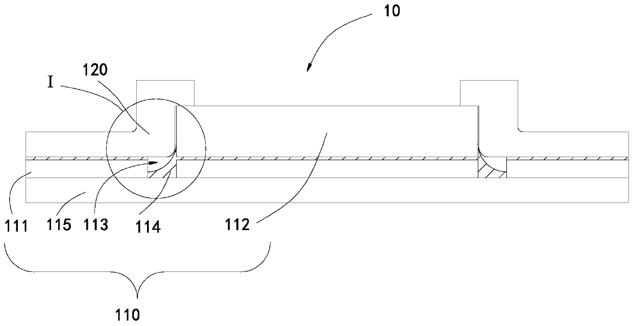
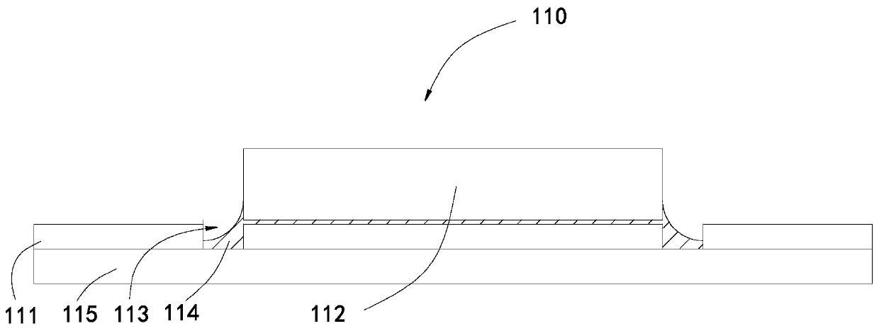
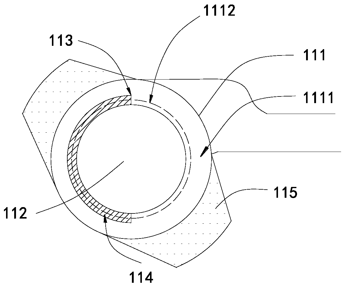
[0035] Embodiments of the present invention are described in detail below, examples of which are shown in the drawings, wherein the same or similar reference numerals denote the same or similar elements or elements having the same or similar functions throughout. The embodiments described below by referring to the figures are exemplary only for explaining the present invention and should not be construed as limiting the present invention.

[0036] In describing the present invention, it should be understood that the terms "center", "longitudinal", "transverse", "length", "width", "thickness", "upper", "lower", "front", " Orientation indicated by rear, left, right, vertical, horizontal, top, bottom, inside, outside, clockwise, counterclockwise, etc. The positional relationship is based on the orientation or positional relationship shown in the drawings, which is only for the convenience of describing the present invention and simplifying the description, rather than indicating ...


PUM


Abstract

The embodiment of the invention provides a circuit board, electronic equipment and a package method, belongs to the field of semiconductor package. The circuit board comprises a substrate, wherein aninstallation surface of the substrate comprises an installation region, an electronic component is arranged on the installation region, a groove is formed in boundary of the installation region and isfilled with filling glue, a part of filling glue is arranged in the groove, and the other part of filling glue is exposed out of the installation surface and is in contact with the electronic component. A cover body of the electronic equipment is arranged at an opening of the groove, and the bending radius of a bending part is smaller than the width of the groove. A part of filling glue is arranged in the groove, the other part of filling glue is exposed out of the installation surface, the volume of the filling glue arranged on a surface of the substrate also can be reduced, thus, the volumeof the cover body can be further reduced, and the volume of the electronic equipment is reduced; and moreover, the bending part of the cover body is arranged at the opening of the groove, the volumeof the bending part of the cover body can be not too small, and insufficient strength of the bending part caused by excessively small volume of the bending part is prevented.

Description

technical field [0001] The invention relates to semiconductor packaging, in particular to a circuit board, electronic equipment and a packaging method. Background technique [0002] After the chip is mounted on the circuit board, it is necessary to fill the gap between the circuit board and the chip with a filler to avoid failure of the solder joint between the circuit board and the chip. However, when mounting decorative parts such as metal rings on the circuit board and wrapping the chips, the decorative parts need to avoid filling glue to avoid the structural interference of the filling glue on the decorative parts, resulting in excessive volume of the decorative parts, which is not conducive to the miniaturization of the circuit board design. Contents of the invention [0003] The invention provides a circuit board, electronic equipment and packaging method to overcome the above-mentioned defects. [0004] In a first aspect, an embodiment of the present invention pro...

Claims


Application Information

Patent Timeline
Patent Type & Authority Patents(China)
IPC IPC(8): H05K1/18
Inventor 苏建斌
Owner GUANGDONG OPPO MOBILE TELECOMM CORP LTD
Why Eureka
Try Eureka