Memory programming device

A memory and processor technology, applied in the direction of instruments, electrical digital data processing, calculation, etc., can solve inconvenient problems and achieve the effect of simplifying the sintering process

Inactive Publication Date: 2018-01-30
ANHUI WANTONG POSTS & TELECOMM CO LTD
View PDF10 Cites 0 Cited by
  • Summary
  • Abstract
  • Description
  • Claims
  • Application Information

AI Technical Summary

Problems solved by technology

This programming method needs to reserve a jumper cap, and there is a process of plugging and unplugging the jumper cap, which is not very convenient

Method used


Image

  • Memory programming device
  • Memory programming device
  • Memory programming device

Examples


Embodiment Construction

[0014] The present invention will be further described below in conjunction with accompanying drawing:

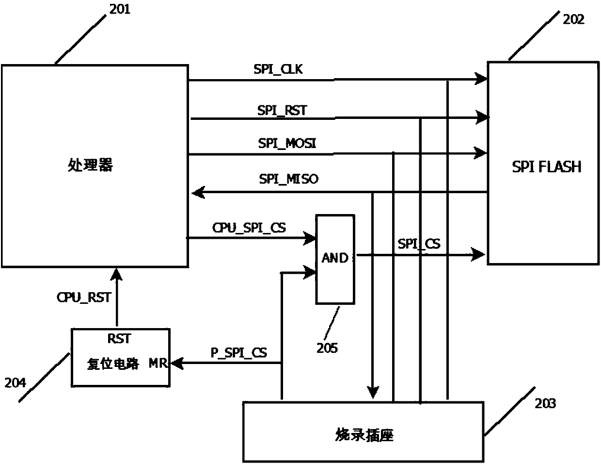
[0015] Such as figure 2 As shown, a memory programming device in this embodiment includes a processor 201 , an SPI Flash chip 202 , a programming socket 203 , a reset circuit 204 , and a driving circuit 205 . The signals related to programming defined on the programming socket 203 include: chip select signal P_SPI_CS, reset signal SPI_RST, clock signal SPI_CLK, data signals SPI_MISO, SPI_MOSI. These signals on the programming socket 203 are connected to the corresponding pins of the SPI Flash 202, and the corresponding signals on the processor 201 are also connected to the SPI Flash. When the board is working normally, the programming cable is not connected to the programming socket, the signal on the programming socket is suspended, and the SPI Flash pin is driven by the processor 201 . When plugging in the cable and burning the SPI Flash, the processor 201 is reset by ...


PUM


Abstract

The invention discloses a memory programming device. Through the memory programming device, a jumper cap is not needed during programming through a simple and ingenious circuit. The memory programmingdevice comprises a processor, an SPI Flash chip, a programming socket, a reset circuit and a driving circuit, wherein a boot code of the processor is stored in the SPI Flash chip, the programming socket is connected with a programming cable to realize programming of the SPI Flash chip, the reset circuit and the driving circuit automatically recognize whether a single board is in a programming state, and if the single board is in the programming state, the processor is reset to avoid influences on programming. According to the memory programming device, a Flash on the single board can be programmed just by plugging in a sintered cable, it is not needed to plug in or out of the jumper cap, the programming process is simplified, and the device is convenient to use and practical.

Description

technical field [0001] The invention relates to the field of circuit design, in particular to a memory burning device. Background technique [0002] Non-volatile storage devices such as SPI Flash, nand Flash, Nor flash, etc. are usually used on the circuit board to store configuration information, Boot code, etc. In the development and debugging stage of the single board, it is necessary to repeatedly program the Flash. Some processors can burn external Flash through online programming methods such as serial ports and USB ports, but most processors do not have such a function, so a convenient and reliable method for Flash programming is required during board debugging . There are two commonly used burning methods at the current stage. The first is to solder the Flash chip socket on the board, put the Flash chip on a dedicated programmer for programming, and then put the chip into the socket to guide the board to start after programming. Plugging and unplugging the socket...

Claims


Application Information

Patent Timeline
Patent Type & Authority Applications(China)
IPC IPC(8): G06F8/654
Inventor 余加兵
Owner ANHUI WANTONG POSTS & TELECOMM CO LTD
Why Eureka
Try Eureka