Supercharge Your Innovation With Domain-Expert AI Agents!

Organic electroluminescence display panel and manufacturing method thereof

An electroluminescent display and display panel technology, applied in circuits, electrical components, electrical solid devices, etc., can solve the problem of uneven brightness at the edge of organic electroluminescent devices, and achieve the effect of improving uneven brightness.

Active Publication Date: 2018-02-16
WUHAN CHINA STAR OPTOELECTRONICS SEMICON DISPLAY TECH CO LTD
View PDF7 Cites 1 Cited by
  • Summary
  • Abstract
  • Description
  • Claims
  • Application Information

AI Technical Summary

Problems solved by technology

[0004] In order to solve the above-mentioned problems in the prior art, the object of the present invention is to provide an organic electroluminescent display panel and its manufacturing method that can eliminate the unevenness of the edge luminous brightness of the organic electroluminescent device.

Method used


Image

  • Organic electroluminescence display panel and manufacturing method thereof
  • Organic electroluminescence display panel and manufacturing method thereof
  • Organic electroluminescence display panel and manufacturing method thereof

Examples


Embodiment Construction

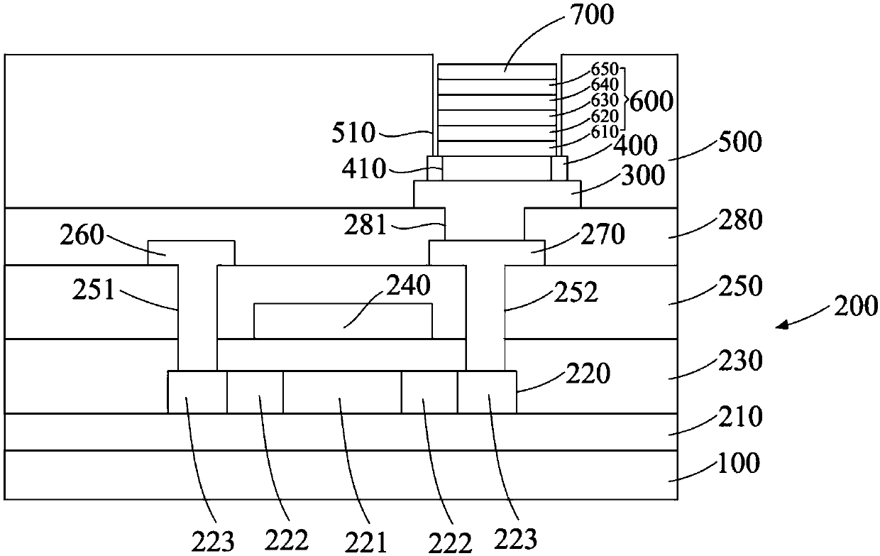
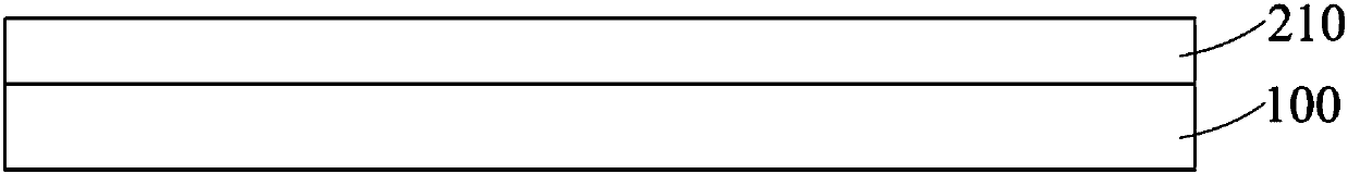
[0019] Hereinafter, embodiments of the present invention will be described in detail with reference to the accompanying drawings. This invention may, however, be embodied in many different forms and should not be construed as limited to the specific embodiments set forth herein. Rather, the embodiments are provided to explain the principles of the invention and its practical application, thereby enabling others skilled in the art to understand the invention for various embodiments and with various modifications as are suited to particular intended uses.

[0020] In the drawings, the thicknesses of layers and regions are exaggerated for device clarity. Like reference numerals refer to like components throughout the specification and drawings.

[0021] It will be understood that when an element such as a layer, film, region, or substrate is referred to as being "on" another element, it can be directly on the other element or intervening elements may also be present. Alternativ...


PUM


Abstract

The invention provides an organic electroluminescence display panel. The organic electroluminescence display panel comprises a substrate, a thin film transistor, a bottom electrode, a shading layer, apixel limiting layer, an organic electroluminescence device and a top electrode, wherein the thin film transistor is arranged on the substrate; the bottom electrode is arranged on a drain electrode of the thin film transistor; the shading layer is arranged on the bottom electrode, a first via hole is formed in the shading layer, and the via hole is exposed out of the bottom electrode; the pixel limiting layer is arranged on the thin film transistor, the bottom electrode and the shading layer, a second via hole is formed in the pixel limiting layer, the hole diameter of the second via hole isgreater than that of the first via hole, and the second via hole is completely exposed out of the first via hole; the organic electroluminescence device is arranged on the bottom electrode; and the top electrode is arranged on the organic electroluminescence device. The invention also provides a manufacturing method of the organic electroluminescence display panel. The edge of the organic electroluminescence device is blocked by using the shading layer, so that the phenomenon that the edge luminance of the organic electroluminescence device is non-uniform is improved.

Description

technical field [0001] The invention belongs to the technical field of organic electroluminescence display, and in particular relates to an organic electroluminescence display panel and a manufacturing method thereof. Background technique [0002] In recent years, organic light-emitting diode (Organic Light-Emitting Diode, OLED) display panel has become a very popular emerging flat display panel product at home and abroad, because OLED display panel has self-illumination, wide viewing angle, short response time, high luminous efficiency, It has the characteristics of wide color gamut, thin thickness, large-size and flexible display panel and simple manufacturing process, and it also has the potential of low cost. [0003] At present, in the existing OLED display panel, the pixel definition layer (PDL layer) obtained through the processes of coating, exposure, development, and baking of the organic photoresist will appear in a state where the top surface is hydrophobic and th...

Claims


Application Information

Patent Timeline
IPC IPC(8): H01L27/32H01L51/52H01L51/56
CPCH10K59/122H01L27/1248H01L27/1259H01L29/78621H01L29/78675H10K59/126H10K71/13H10K59/1201H10K50/11H10K50/15H10K50/16H10K50/17H10K50/81H10K50/82H10K50/85H10K50/86H10K50/171H10K59/12H10K71/00
Inventor 李松杉
Owner WUHAN CHINA STAR OPTOELECTRONICS SEMICON DISPLAY TECH CO LTD
Features
  • R&D
  • Intellectual Property
  • Life Sciences
  • Materials
  • Tech Scout
  • Unparalleled Data Quality
  • Higher Quality Content
  • 60% Fewer Hallucinations
Learn More