Method for manufacturing circuit board

A manufacturing method and circuit board technology, which are applied in the direction of printed circuit manufacturing, printed circuit, and electrical connection formation of printed components, etc., can solve the problem of uneven desmear removal effect, poor desmear removal effect, and poor contact area of ​​potassium permanganate And so on, to achieve the effect of uniform desmear removal, good desmear effect and sufficient desmear effect

Active Publication Date: 2018-02-16
重庆市志益鑫电子科技有限公司
View PDF5 Cites 0 Cited by
  • Summary
  • Abstract
  • Description
  • Claims
  • Application Information

AI Technical Summary

Problems solved by technology

[0005] However, there are still certain problems in the above-mentioned technical scheme: when desmearing, only the rigid hanging basket of the substrate that needs to be desmeared is directly sunk into the casing, and the desmearing is carried out by potassium permanganate desmearing agent. However, this method will lead to different contact areas between the substrate and potassium permanganate at various positions in the hanging basket, and the effect of removing smear is not uniform. The substrate does not fully react with potassium permanganate, and the effect of removing smear is not good

Method used


Image

  • Method for manufacturing circuit board

Examples


Embodiment 1

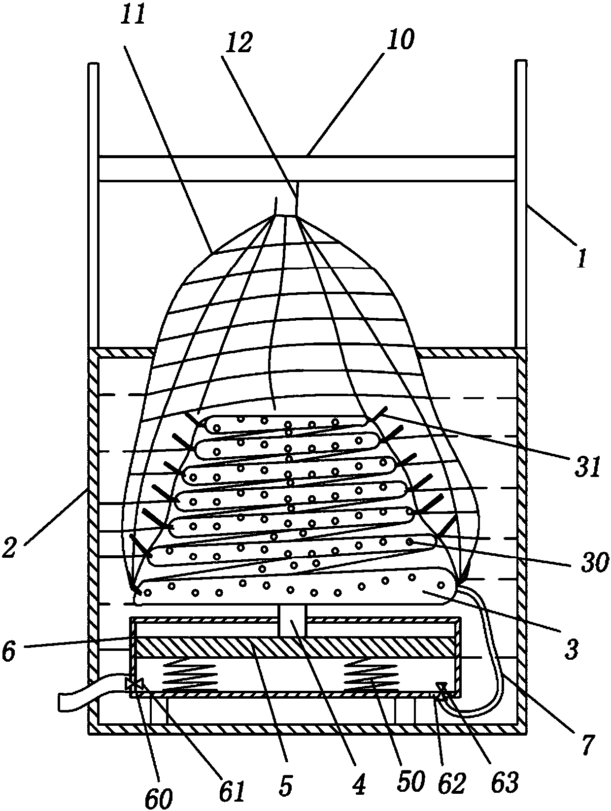
[0030] The embodiment is basically as attached figure 1 Shown: circuit board manufacturing method, comprises the following steps:

[0031] A. Putting on the shelf: put the substrate that needs to be desmeared into the hanging basket, and fix the hanging basket on the walking frame 10 with a hook 12; the hanging basket is a flexible mesh basket 11; a deformable net made of PVC material is preferred Shape basket 11, walking frame 10 is vertically slidably connected with frame 1.

[0032] B. Leavening: Put the mesh basket into the medicine tank with leavening agent and react for 3 minutes.

[0033] C. Water washing: wash the bulky substrate with deionized water, and wash twice.

[0034] D, glue removal: put the mesh basket into the glue removal device, and react for 1min; the glue removal device includes a casing 2 for loading glue remover, and the glue remover is preferably potassium permanganate solution in the present embodiment , the box body 2 is provided with a support c...

Embodiment 2

[0043] The difference between this embodiment and embodiment 1 is:

[0044] The bulking reaction time in step B is 2 minutes; the reaction time for desmearing in step D is 3 minutes; the neutralization reaction time in step F is 3 minutes.

Embodiment 3

[0046] The difference between this embodiment and embodiment 1 is:

[0047] The bulking reaction time in step B is 3 minutes; the reaction time for removing smear in step D is 5 minutes; the neutralization reaction time in step F is 3 minutes.


PUM


Abstract

The invention belongs to the technical field of electronic devices, in particular to a method for manufacturing a circuit board, which comprises the following steps: A, putting on the shelf: putting the substrate which needs smear removal into a hanging basket and fixing the hanging basket on a traveling shelf, wherein the hanging basket is a flexible mesh basket; B, bulking: placing the mesh basket into a medicine tank filled with a raising agent for reaction of 1 to 3 min; C, washing: washing the bulked substrate with deionized water; D, smear removal: placing the mesh basket into a smear removal device for reaction of 1 to 5 min, wherein the smear removal device includes a container for loading a glue removal agent, the container is internally provided with a support column, a piston, acylinder, a hose and a coiler; E, washing with water: washing the substrate subjected to the smear removal with deionized water; F, and neutralization: placing the mesh basket into the medicine tankfilled with a neutralizer for reaction of 2 to 3 min; and G, washing: washing the neutralized substrate with deionized water. The technical solution can enable the substrate to fully react with the glue removal agent and improve the smear removal effect of the substrate.

Description

technical field [0001] The invention belongs to the technical field of electronic devices, and in particular relates to a method for manufacturing a circuit board. Background technique [0002] The circuit board (PCB) is a dry film pasted on the copper clad board, which is exposed, developed and etched to form a conductive circuit pattern, which plays the role of current conduction and signal transmission in electronic products, and is the carrier of electronic components. The production process of PCB is mainly divided into eight parts: inner layer circuit, lamination, drilling, hole metallization, outer layer dry film, outer layer circuit, silk screen, surface process and post process. The purpose of the hole metallization process is to metallize the resin and glass fiber of the non-conductor part on the hole wall, so as to facilitate the subsequent electroplating process and provide a metal hole wall with sufficient conductivity and protection; the hole metallization proc...

Claims


Application Information

Patent Timeline
Patent Type & Authority Applications(China)
IPC IPC(8): H05K3/42
CPCH05K3/42H05K2203/0766H05K2203/0796
Inventor 胡红生
Owner 重庆市志益鑫电子科技有限公司
Why Eureka
Try Eureka