Printed circuit board (PCB) design method for preventing electromagnetic interference (EMI)

A PCB board, design method technology, applied in the direction of crosstalk/noise/electromagnetic interference reduction (, circuit devices, printed circuit components, etc., can solve the problems of wasting assembly time, products with EMI grounding points, few contact points, etc., Achieve the effect of solving the EMI problem

Inactive Publication Date: 2018-02-23
ZHENGZHOU YUNHAI INFORMATION TECH CO LTD
View PDF5 Cites 0 Cited by
  • Summary
  • Abstract
  • Description
  • Claims
  • Application Information

AI Technical Summary

Problems solved by technology

[0004] In order to prevent the occurrence of EMI problems, sufficient grounding of the PCB board and the metal case can effectively prevent the occurrence of EMI problems, but the PCB board is fixed by locking screws, and only the screw holes are connected to the ground of the case. There are relatively few points, and there is often no way to completely solve the EMI problem
[0005] On the other hand, under normal circumstances, when the PCB board is assembled, it is fixed and assembled by locking screws. However, because there are many screws fixed, the PCB board assembly takes a lot of time.
[0006] In view of the above situation, this application invented a PCB board design method to prevent EMI, which can effectively solve the EMI problem of some products and the problem that the PCB board is assembled by locking screws with few grounding points and wastes assembly time.

Method used


Image

  • Printed circuit board (PCB) design method for preventing electromagnetic interference (EMI)
  • Printed circuit board (PCB) design method for preventing electromagnetic interference (EMI)
  • Printed circuit board (PCB) design method for preventing electromagnetic interference (EMI)

Examples


Embodiment Construction

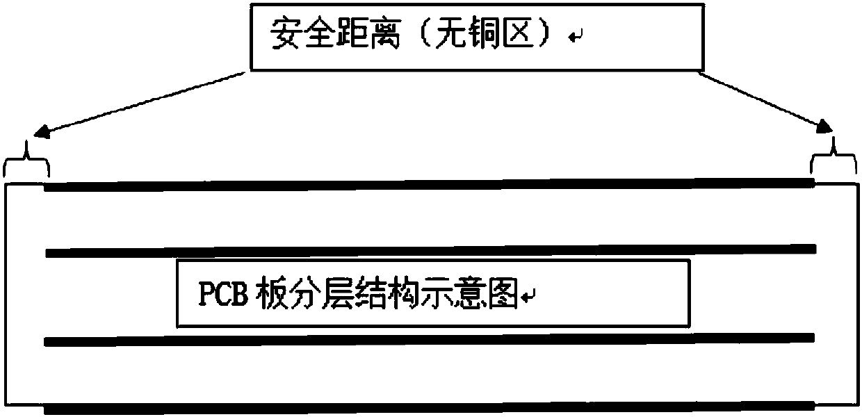
[0018] as attached figure 1 As shown, the metal shell electronic products in the prior art are usually fixed by locking screws when assembling the PCB, and in order to prevent short circuit caused by copper leakage at the edge of the PCB, the edge of the PCB, whether it is the inner layer or the outer layer, cannot With copper foil. Therefore, the current PCB design needs to keep a safe distance.

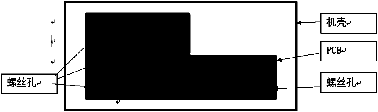
[0019] as attached figure 2 As shown, the existing PCB board fixing method is to lock the screw and fix it by locking the screw.

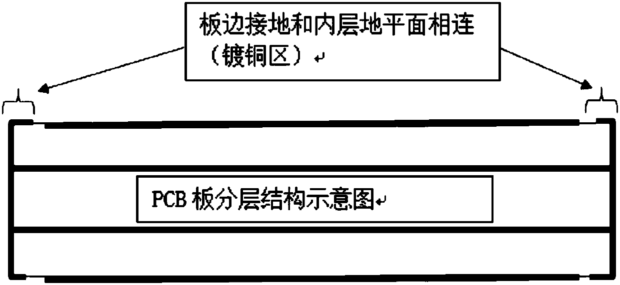
[0020] In the present invention, grounding copper is leaked from the edge of the PCB board, and the copper plating on the edge of the board is grounded. When assembling, the copper plating on the edge of the board and the metal casing are directly contacted and clamped to achieve the purpose of direct fixing, which not only saves the time of locking screws but also can It has a better effect of preventing EMI.

[0021] The specific implementation st...


PUM


Abstract

The invention relates to the field of circuit design, in particular to a printed circuit board (PCB) design method for preventing electromagnetic interference (EMI). According to the method, a PCB edge is plated with copper, is connected with ground and is directly clamped and connected with an enclosure, the grounding connection area is expanded, a better EMI-prevention effect is achieved, meanwhile, the time of screw locking is saved, the manual cost is indirectly reduced, and the production efficiency is improved.

Description

technical field [0001] The invention relates to the field of circuit design, in particular to a PCB board design method for preventing EMI. This method directly clamps and connects the copper-plated grounding of the PCB board and the chassis, which improves the grounding connection area and achieves a better effect of preventing EMI. At the same time, it saves the time of locking screws, indirectly saves labor costs, and improves production efficiency. . Background technique [0002] With the increasing complexity of electronic systems, EMI (Electromagnetic Interference, electromagnetic interference) problems are also increasing. In order to make their products meet the relevant international standards, designers have to go back and forth between the office and the EMC laboratory to repeatedly test, modify the design, and test again. This not only wastes manpower and material resources, but also delays the time to market of the product, and brings immeasurable losses to th...

Claims


Application Information

Patent Timeline
IPC IPC(8): H05K1/02
CPCH05K1/0215
Inventor 周冬
Owner ZHENGZHOU YUNHAI INFORMATION TECH CO LTD
Why Eureka
Try Eureka