Supercharge Your Innovation With Domain-Expert AI Agents!

Phase shift mask

A technology of phase shifting and photomask, which is applied in the direction of optics, photographic process of pattern surface, and originals for photomechanical processing, etc. It can solve the problems of limited protection and limited elasticity of light-transmitting substrates

Active Publication Date: 2018-03-09
TAIWAN SEMICON MFG CO LTD
View PDF9 Cites 0 Cited by
  • Summary
  • Abstract
  • Description
  • Claims
  • Application Information

AI Technical Summary

Problems solved by technology

However, existing chromium-free phase-shift photomasks are limited in their flexibility to improve image quality and other issues, such as the tolerance of the etch process relative to the expected phase shift
In addition, the existing chromium-free phase-shift photomasks have limited protection for the light-transmitting substrate when forming and using the photomask.

Method used


Image

  • Phase shift mask
  • Phase shift mask
  • Phase shift mask

Examples


Embodiment Construction

[0040] It should be understood that different embodiments or examples provided below may implement different structures of various embodiments. The examples of specific components and arrangements are used to simplify the invention and not to limit the invention. In addition, numbers may be repeated in various examples of the present invention, but these repetitions are only for simplification and clarity of description, and do not mean that units with the same numbers in different embodiments and / or arrangements have the same corresponding relationship.

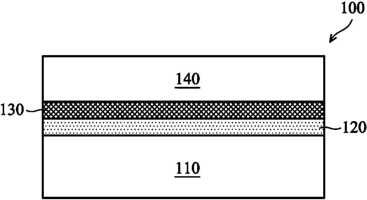
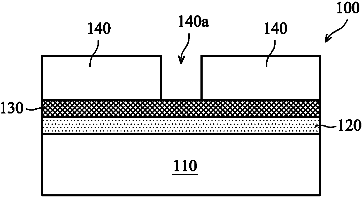
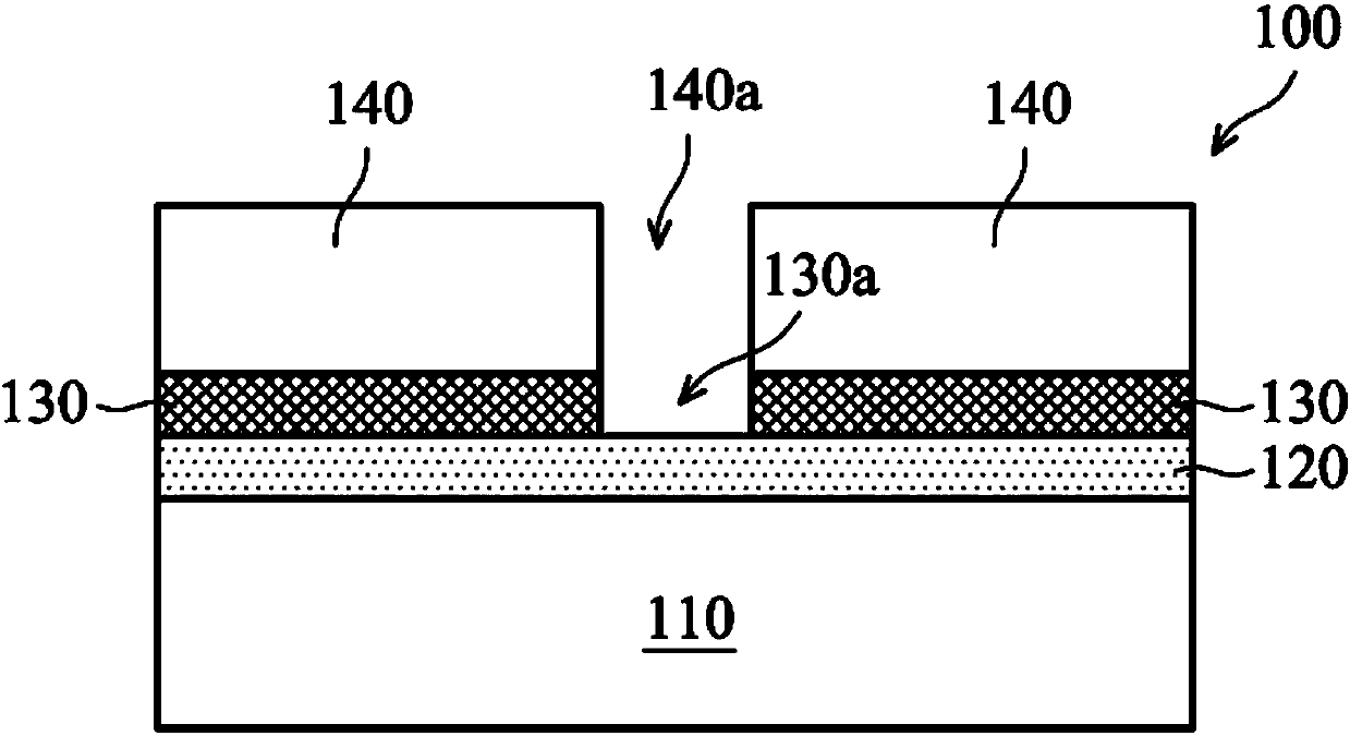
[0041] Figures 1 to 4 is a cross-sectional view of photomask 100 in some embodiments of the present invention. Figure 5 is some examples, Figure 4 Top view of photomask 100. Figures 1 to 5 The photomask 100 and its method of forming are described. The photomask 100 defines a circuit pattern thereon, and the circuit pattern can be transferred to the semiconductor substrate by radiation (such as light beam) in a lithog...


PUM

PropertyMeasurementUnit
thicknessaaaaaaaaaa
thicknessaaaaaaaaaa
transmittivityaaaaaaaaaa

Abstract

The present disclosure provides a phase shift mask. The phase shift mask includes a transparent substrate; an etch stop layer disposed on the substrate; and a tunable transparent material layer disposed on the etch stop layer and patterned to have an opening, wherein the tunable transparent material layer is designed to provide phase shift and has a transmittance greater than 90%.

Description

technical field [0001] Embodiments of the present invention relate to a method for forming a semiconductor structure, and more particularly relate to a phase shift photomask used therefor. Background technique [0002] In semiconductor technology, optical interference and other effects often cause variations in critical dimensions. As such, the photomask error parameters would be unacceptably high for the size of the smaller structures in sub-wavelength patterning, especially contact holes. Various techniques have been used to improve photomask error parameters, such as using phase-shift photomasks (eg, chrome-free phase-shift photomasks) to define circuit patterns. In the chrome-free phase-shift photomask, the circuit structure is defined in the light-transmitting photomask, and there is a phase shift between adjacent light-transmitting regions of the transparent photomask. As such, when imaged onto a semiconductor substrate, destructive interference will produce dark str...

Claims


Application Information

Patent Timeline
Patent Type & Authority Applications(China)
IPC IPC(8): G03F1/26
CPCG03F1/26G03F1/34G03F1/80G03F1/38H01L21/266
Inventor 林云跃李信昌
Owner TAIWAN SEMICON MFG CO LTD
Features
  • R&D
  • Intellectual Property
  • Life Sciences
  • Materials
  • Tech Scout
  • Unparalleled Data Quality
  • Higher Quality Content
  • 60% Fewer Hallucinations
Learn More