

SOI material with nitride film as insulating buried layer and preparation method thereof
A technology of insulating buried layer and silicon nitride thin film, which is applied in semiconductor/solid-state device manufacturing, electrical components, circuits, etc., can solve problems such as cracking and inapplicable SOI material preparation, and achieve reducing internal stress, increasing quality, Effect of reducing warpage variation
- Summary
- Abstract
- Description
- Claims
- Application Information
AI Technical Summary
Problems solved by technology
Method used
Image

Examples
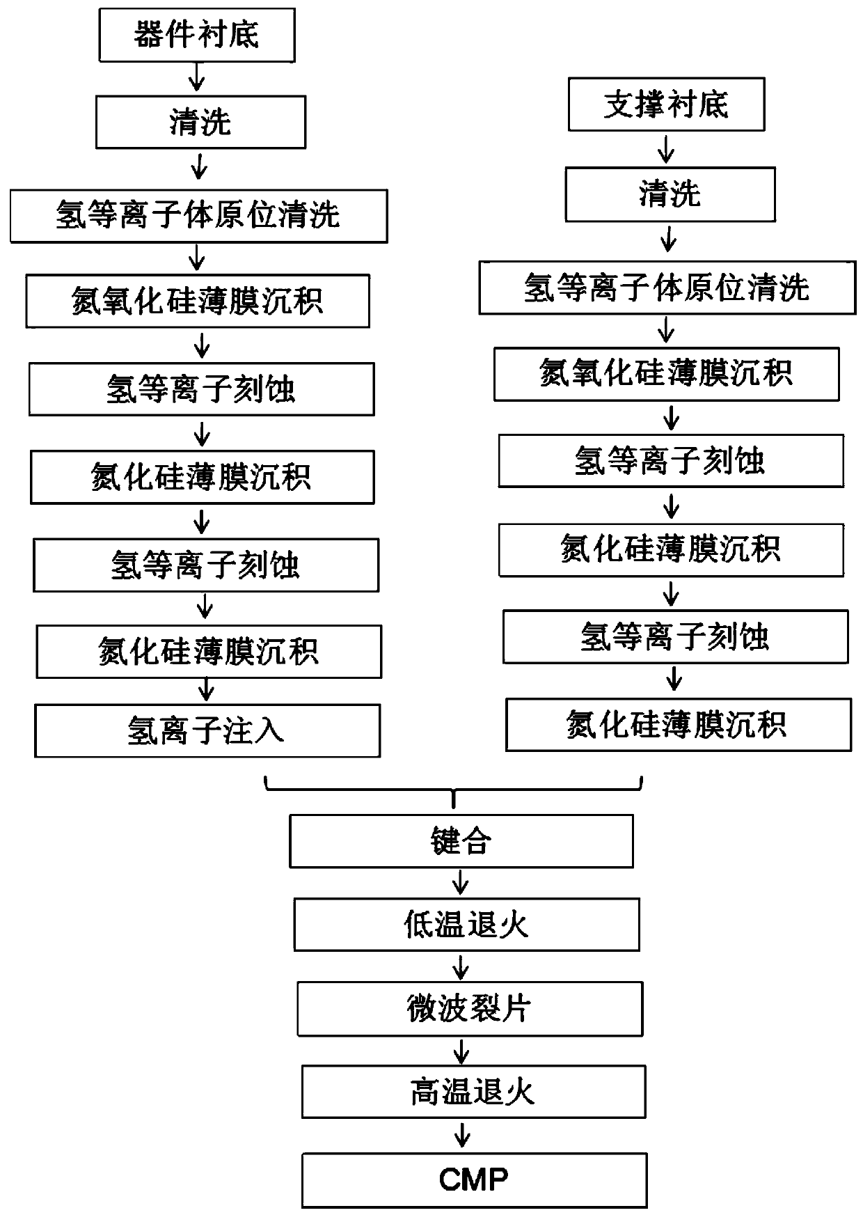
Embodiment 1
[0027] This embodiment is to prepare the SOI material forming the top layer silicon film / silicon oxynitride film / silicon nitride film / silicon oxynitride film / silicon substrate, and the thickness of each layer is 20nm / 10nm / 60nm / 10nm / 725μm respectively. Specific steps are as follows:
[0028] 1) Use 8-inch P-type silicon wafers with a resistivity of 8.5-11.5ohm.cm, crystal orientation , and a thickness of 725μm as the device substrate and supporting substrate.
[0029] 2) Use HF, H in turn 2 SO 4 and H 2 o 2 The mixed solution and deionized water were used to ultrasonically clean the device substrate and the support substrate successively, and put them into the reaction chamber of the PECVD equipment after being dried.
[0030] 3) The device substrate and the support substrate are cleaned in situ by hydrogen plasma, the flow rate of hydrogen gas is 50 sccm, and the cleaning time is 20 minutes.
[0031] 4) Depositing a silicon oxynitride film on the device substrate or the s...
Embodiment 2
[0042] This example is to prepare the SOI material forming the top layer silicon film / silicon oxynitride film / silicon nitride film / silicon oxynitride film / silicon substrate, and the thickness of each layer is 13.5 μm / 0.5 μm / 4 μm / 0.5nm / 675 μm . Specific steps are as follows:
[0043] 1) Select a 6-inch N-type silicon wafer with a resistivity of 4-7ohm.cm, crystal orientation , and a thickness of 675 μm as the device substrate and supporting substrate.
[0044] 2) Use HF, H in turn 2 SO 4 and H 2 o 2 The mixed solution and deionized water were used to ultrasonically clean the device substrate and the support substrate successively, and put them into the reaction chamber of the PECVD equipment after being dried.
[0045] 3) The device substrate and the supporting substrate are cleaned in situ by hydrogen plasma, the flow rate of hydrogen gas is 70 sccm, and the cleaning time is 15 minutes.
[0046] 4) Depositing a silicon oxynitride film on the device substrate or the suppo...
PUM
| Property | Measurement | Unit |
|---|---|---|
| thickness | aaaaa | aaaaa |
| thickness | aaaaa | aaaaa |
| thickness | aaaaa | aaaaa |
Abstract
Description
Claims
Application Information