Warpage control method of silicon substrate material for gan epitaxy

A control method and technology for silicon substrates, which are used in semiconductor/solid-state device manufacturing, semiconductor devices, electrical components, etc., can solve the problems of large thermal expansion coefficient, large wafer warpage, and high lattice mismatch rate, and reduce a large number of The incidence of defects and the effect of reducing the warpage variation of silicon wafers

Active Publication Date: 2018-11-23
杭州中欣晶圆半导体股份有限公司
View PDF2 Cites 0 Cited by
  • Summary
  • Abstract
  • Description
  • Claims
  • Application Information

AI Technical Summary

Problems solved by technology

[0003] Although the Si substrate has the advantages of low substrate raw material cost and large substrate heat dissipation coefficient compared with other materials, it also has some negative effects, such as: high lattice mismatch rate, large thermal expansion coefficient, and generation Cracks and large wafer warpage during high temperature epitaxy

Method used


Image

  • Warpage control method of silicon substrate material for gan epitaxy
  • Warpage control method of silicon substrate material for gan epitaxy
  • Warpage control method of silicon substrate material for gan epitaxy

Examples


Embodiment Construction

[0010] The method for controlling the warpage of the silicon substrate material for GaN epitaxy according to the present invention will be further described in detail below in conjunction with the accompanying drawings.

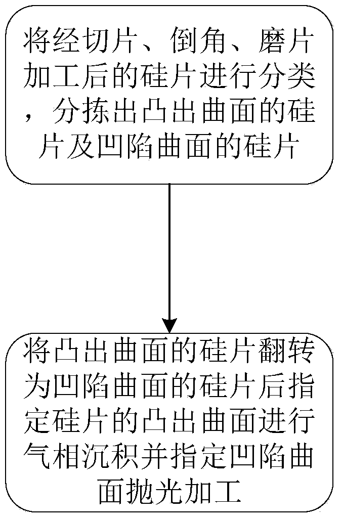
[0011] Such as figure 1 As shown, the method for controlling the warpage of silicon substrate materials for GaN epitaxy in the present invention first classifies the silicon wafers processed by slicing, chamfering and grinding, and sorts out the silicon wafers with convex curved surface (+BOW) And the silicon wafer with concave surface (-BOW), then turn the silicon wafer with convex surface into the silicon wafer with concave surface, and then specify the convex surface of the silicon wafer for vapor deposition and specify the concave surface polishing process.

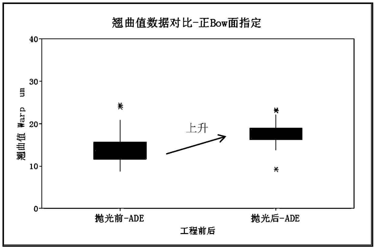
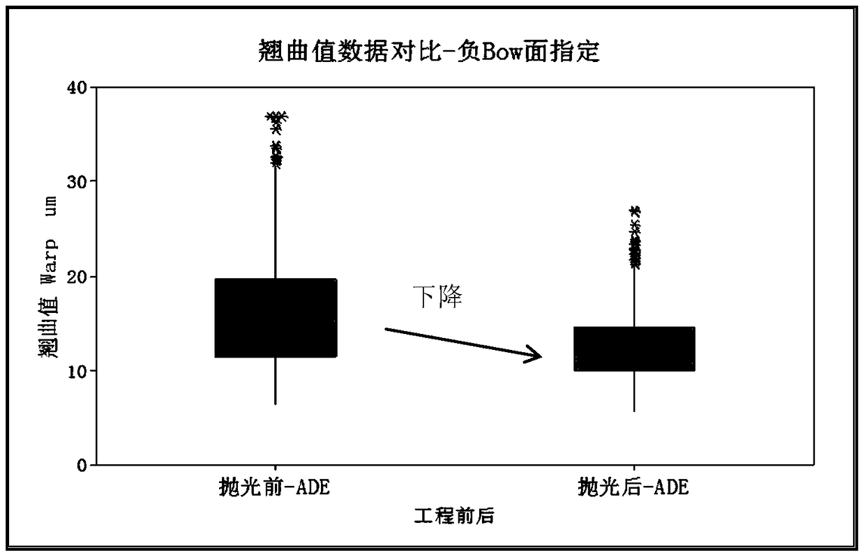
[0012] figure 2 It is: designate the concave curved surface as the vapor deposition surface, and designate the convex curved silicon wafer as the polished surface to change the warpage data before ...


PUM


Abstract

The invention relates to a warping degree control method for silicon substrate materials for GaN epitaxies. The warping degree control method includes the following steps: (1) silicon wafers obtained after slicing, chamfering and grinding are classified, and the silicon wafers with convex curve faces and the silicon wafers with concave curve faces are sorted out; (2) the silicon wafers with the convex curve faces are overturned to be the silicon wafers with the concave curve faces, vapor deposition is carried out on specified convex curve faces of the silicon wafers, and specified concave faces are polished. By means of the warping degree control method for the silicon substrate materials for the GaN epitaxies, silicon wafer warping changes caused during GaN epitaxy growth can be effectively reduced, and therefore the large-quantity unqualified product occurrence rate caused after GaN epitaxy growth is carried out is reduced.

Description

technical field [0001] The invention belongs to the field of semiconductor manufacturing, and relates to the technical research and development of silicon substrate materials for GaN epitaxy, in particular to a method for controlling the warpage of silicon substrate materials for GaN epitaxy. Background technique [0002] The research and application of GaN materials is the third-generation semiconductor material for the development of new semiconductors for microelectronic devices and optoelectronic devices. GaN epitaxial substrates are commonly Si / SiC / Al 2 o 3 , and compared with the advantages of low raw material cost of Si substrate, large substrate heat dissipation coefficient, and large-size silicon substrate can be tried for research and development. [0003] Although the Si substrate has the advantages of low substrate raw material cost and large substrate heat dissipation coefficient compared with other materials, it also has some negative effects, such as: high la...

Claims


Application Information

Patent Timeline
Patent Type & Authority Patents(China)
IPC IPC(8): H01L33/00H01L21/02
CPCH01L21/02035H01L33/00
Inventor 宋玮贺贤汉金文明
Owner 杭州中欣晶圆半导体股份有限公司
Why Eureka
Try Eureka