Cover glass for solid imaging device, and its manufacturing method

A technology of solid-state imaging elements and manufacturing methods, applied in the fields of electric solid-state devices, electrical components, semiconductor devices, etc.

Active Publication Date: 2007-07-04
NIPPON ELECTRIC GLASS CO LTD
View PDF4 Cites 1 Cited by
  • Summary
  • Abstract
  • Description
  • Claims
  • Application Information

AI Technical Summary

Problems solved by technology

[0011] In addition, especially in the cleanliness of a cover glass for a solid-state imaging device in which a thin film is formed on the glass surface, there is a problem that the periphery of the film peels off due to the passage of time after t

Method used


Image

  • Cover glass for solid imaging device, and its manufacturing method
  • Cover glass for solid imaging device, and its manufacturing method
  • Cover glass for solid imaging device, and its manufacturing method

Examples


Embodiment Construction

[0095] Hereinafter, the cover glass for solid-state imaging devices which concerns on embodiment of this invention, and its manufacturing method are demonstrated in detail with reference to drawings.

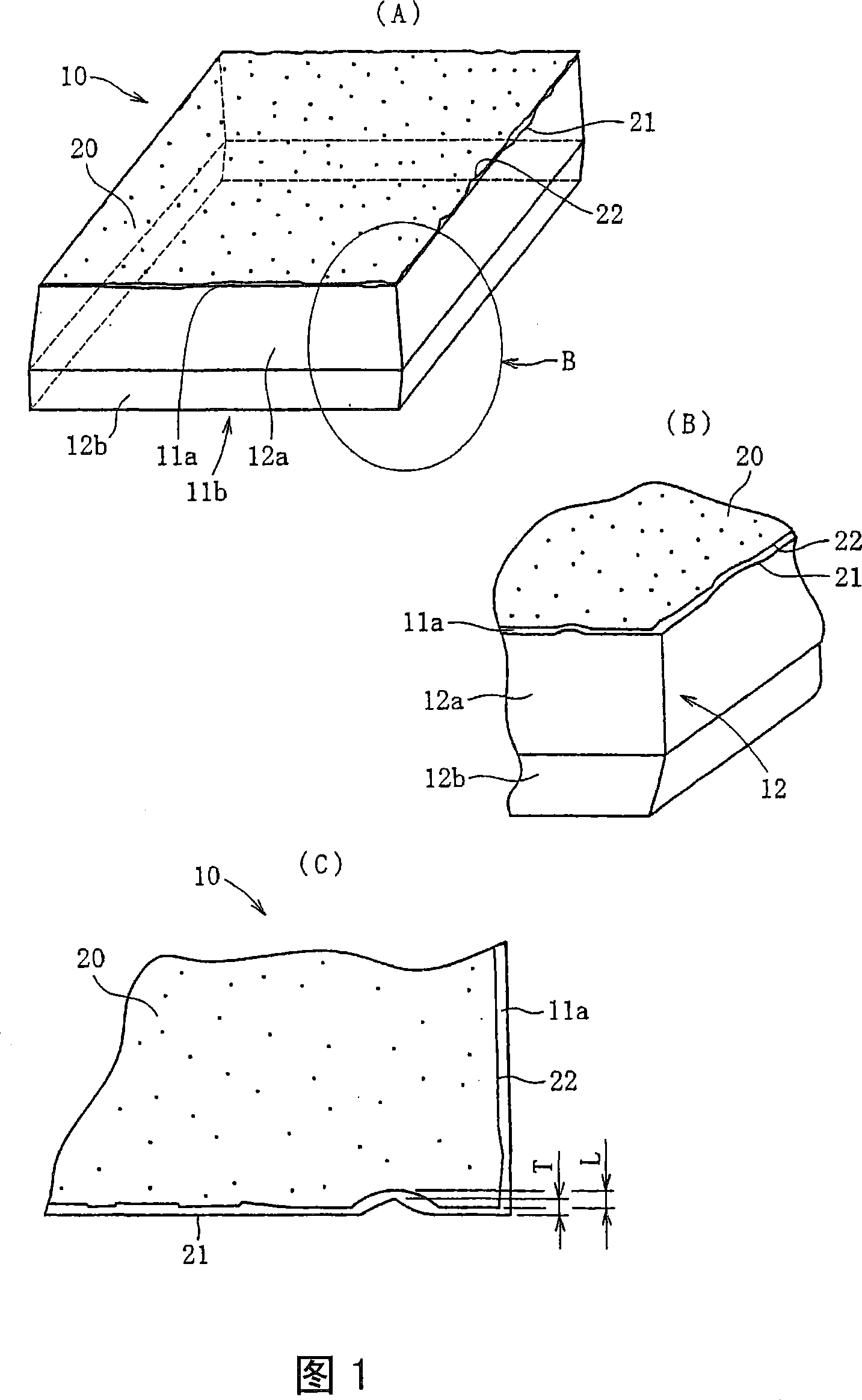
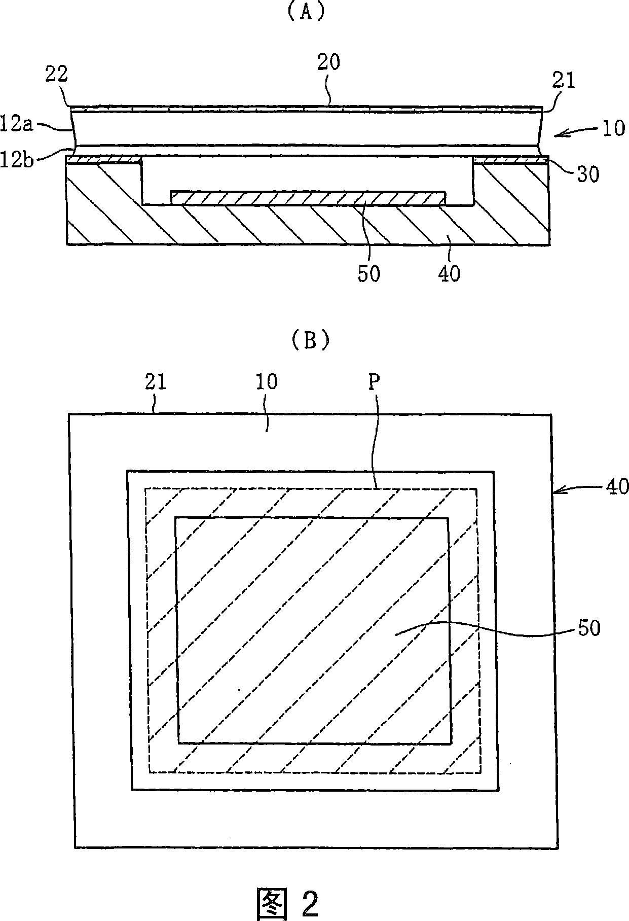
[0096] Fig. 1(A) is a perspective view of a cover glass for a solid-state imaging device according to an embodiment of the present invention, Fig. 1(B) is an enlarged perspective view of a portion indicated by a symbol B in Fig. 1(A), and Fig. 1(C) is the same Partial enlarged top view. 2(A) is a longitudinal sectional front view showing a state in which the above-mentioned cover glass for a solid-state imaging device is mounted on a package for a solid-state imaging device, and FIG. 2(B) is a plan view showing the same state.

[0097] This cover glass 10 for a solid-state imaging device is a cover glass using plate glass (a small plate glass sheet) made of an alkali-free borosilicate glass having 60% of SiO in % by mass. 2 , 14.7% Al 2 o 3 , 11% B 2 o 3 , 3% of RO (RO=MgO+...


PUM

PropertyMeasurementUnit
Lengthaaaaaaaaaa
Thicknessaaaaaaaaaa
Thicknessaaaaaaaaaa

Abstract

Cover glass (10) for solid image pickup device comprising a flat glass plate made of an inorganic oxide glass and, superimposed on the front and back, viewed in the direction of plate thickness, thereof, first translucent plane (11a) and second translucent plane (11b), wherein the first translucent plane (11a) is provided with thin film (20), and wherein an unevenness is provided at extreme edge (22) of the thin film (20) positioned at an outer edge on the first translucent plane (11a) of the flat glass plate, the unevenness having projection dimension (L) ranging from 0.5 to 50 m, the projection dimension (L) defined as extending from, on a plane parallel to the first translucent plane (11a), the most recessed position to the most protrudent position. Such a cover glass is produced through a process comprising the steps of melting a glass raw material mixture in a heat resistant vessel, molding the thus molten glass into a plate glass, providing the plate glass with a thin film and fracturing the plate glass with the thin film into small glass pieces.

Description

technical field [0001] The present invention relates to a cover glass that is arranged as a window material for transmitting light on a package housing a solid-state imaging device and protects the solid-state imaging device, and a method for manufacturing the same. Background technique [0002] CCD (Charge Coupled Device), which is a representative component of solid-state imaging devices, has a relatively early development history. Tubes (or also called vacuum tube imaging elements, image tubes) have been widely used, and their advantages of being small, impact-resistant, and low-power consumption have also been effectively utilized, so they are still widely used today. used in the field. That is, the CCD has overcome the disadvantages of low sensitivity compared with the image pickup tube, and by realizing various functions such as electronic shutter, hand vibration correction, zoom function, etc., it has the performance of replacing the camera that displays the image on...

Claims


Application Information

Patent Timeline
IPC IPC(8): H01L27/14C03C3/091C03C3/093
CPCC03C17/001H01L31/0203C03C14/00
Inventor 中堀宏亮大川大介淀川正弘
Owner NIPPON ELECTRIC GLASS CO LTD
Why Eureka
Try Eureka