LED epitaxial wafer and preparation method thereof

An LED epitaxial wafer and epitaxial growth technology, applied in chemical instruments and methods, crystal growth, electrical components, etc., can solve the problems of insufficient surface flatness of epitaxial wafers and high defect density of epitaxial wafers, and increase antistatic ability, crystal lattice, etc. Good quality, avoid too fast effect

Pending Publication Date: 2022-07-08
JIANGXI ZHAO CHI SEMICON CO LTD
View PDF0 Cites 4 Cited by
  • Summary
  • Abstract
  • Description
  • Claims
  • Application Information

AI Technical Summary

Problems solved by technology

[0004] However, the currently used two-dimensional growth layer is a pure GaN layer, and the temperature and pressure of the two-dimensional growth layer are usually kept constant, resulting in effective defect mitigation of this two-dimensional growth layer, and the defect density of the epitaxial wafer is still high. Epitaxial wafer surface flatness is still insufficient

Method used


Image

  • LED epitaxial wafer and preparation method thereof
  • LED epitaxial wafer and preparation method thereof

Examples


Embodiment 1

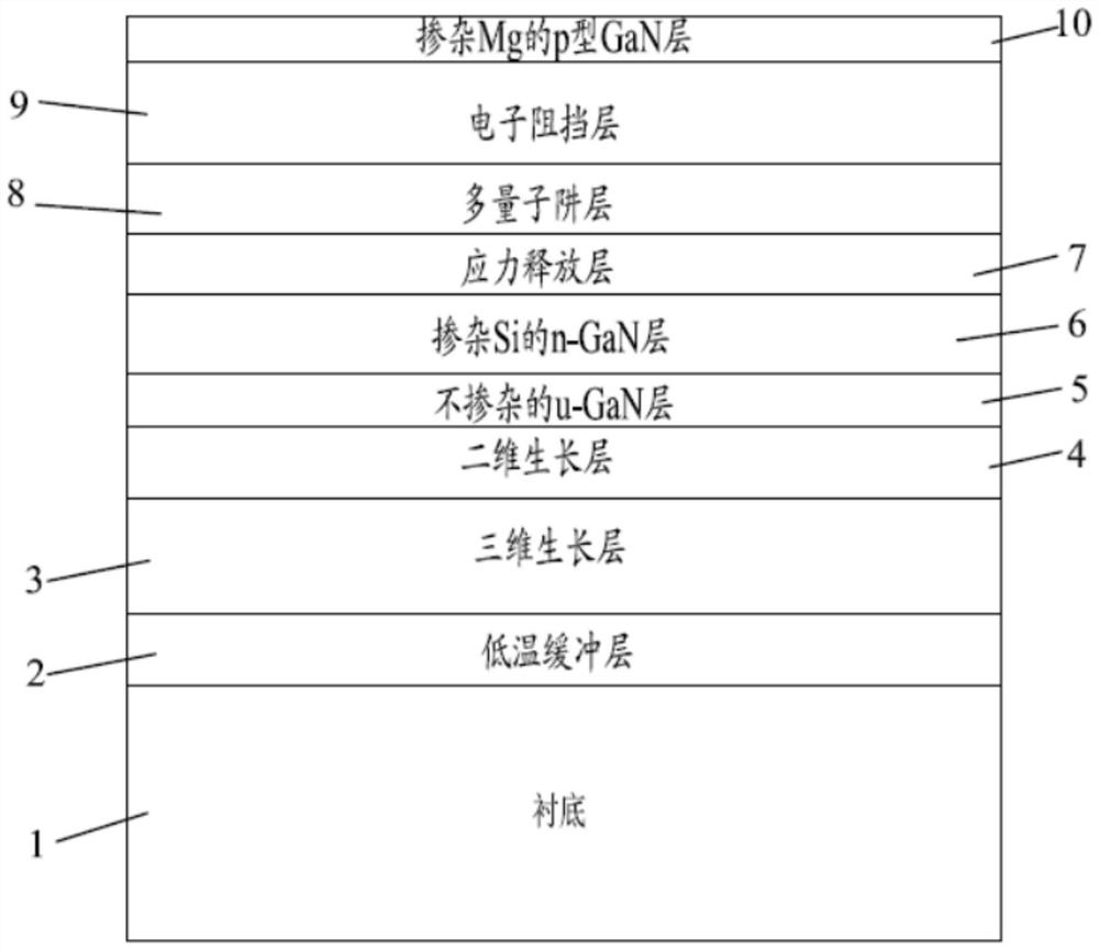
[0036] see figure 1 , shows the LED epitaxial wafer in the first embodiment of the present invention, including a substrate 1, and a low-temperature buffer layer 2, a three-dimensional growth layer 3, a two-dimensional growth layer 4, a GaN layer, a stress Release layer 7 , multiple quantum well layer 8 , electron blocking layer 9 and Mg-doped p-type GaN layer 10 , wherein the GaN layer includes an undoped u-GaN layer 5 sequentially grown on the two-dimensional growth layer 4 And the Si-doped n-GaN layer 6 , a stress relief layer 7 is grown on the Si-doped n-GaN layer 6 .

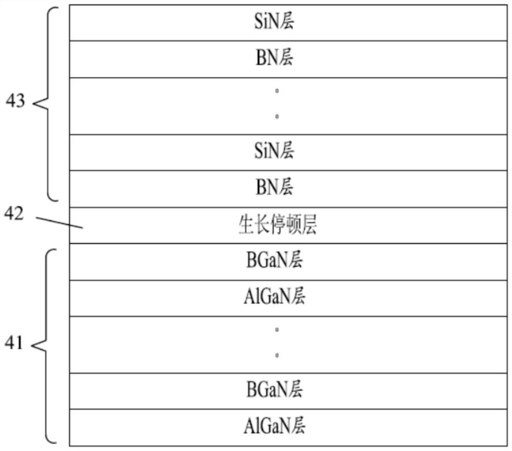
[0037] In this example, see figure 2 , the two-dimensional growth layer 4 includes a first sub-layer 41, a second sub-layer 42 and a third sub-layer 43 grown in sequence; wherein, the first sub-layer 41 is composed of AlGaN layers and BGaN layers that are repeatedly overlapped (alternately stacked) Periodic composite layer, and in the growth cycle of the first sublayer 41, the growth temperature increase...

Embodiment 2

[0042] The second embodiment of the present invention provides a method for preparing an LED epitaxial wafer, which is used for preparing the LED epitaxial wafer in the above-mentioned first embodiment. The method specifically includes steps S21 to S30, wherein:

[0043] Step S21, providing a substrate required for epitaxial growth, preferably a sapphire substrate.

[0044] Specifically, the temperature can be controlled to be 1000 ° C ~ 1200 ° C, at H 2 The substrate is annealed at high temperature for about 5 min under the atmosphere.

[0045] In step S22, a low temperature buffer layer is grown on the substrate, the material of the low temperature buffer layer may be AlGaN, the temperature of the reaction chamber is 500°C to 700°C, and the pressure is 200 to 400 Torr.

[0046] Step S23 , growing a three-dimensional growth layer on the low temperature buffer layer, the temperature of the three-dimensional growth layer reaction chamber is 1000° C.˜1050° C., and the pressure ...


PUM

PropertyMeasurementUnit
Thicknessaaaaaaaaaa

Abstract

The invention provides an LED epitaxial wafer and a preparation method thereof, the LED epitaxial wafer comprises a substrate, and a low-temperature buffer layer, a three-dimensional growth layer, a two-dimensional growth layer and a GaN layer which are grown on the substrate in sequence, and the two-dimensional growth layer comprises a first sub-layer, a second sub-layer and a third sub-layer which are grown in sequence; wherein the first sub-layer is a periodic composite layer formed by repeatedly overlapping an AlGaN layer and a BGaN layer, the second sub-layer is a growth pause layer, and the third sub-layer is a periodic composite layer formed by repeatedly overlapping and growing a BN layer and an SiN layer. According to the LED epitaxial wafer, the two-dimensional growth layer is specially designed, and the composite two-dimensional growth layer is adopted, so that the LED epitaxial wafer which is higher in surface flatness, smaller in dislocation density, better in antistatic capacity, few in defect extending to a quantum well and improved in luminous intensity can be obtained.

Description

technical field [0001] The invention relates to the technical field of light-emitting diodes, in particular to an LED epitaxial wafer and a preparation method thereof. Background technique [0002] LED (Light Emitting Diode, light-emitting diode) is a semiconductor electronic component that can emit light, and is widely used in various fields due to its small size, high brightness, and low energy consumption. Among them, GaN-based LED is a common type of LED, which has been widely used in the field of solid-state lighting and display, attracting more and more people's attention. [0003] However, GaN-based LEDs currently have a fatal defect, that is, there is a large lattice mismatch and thermal mismatch between the GaN layer of the epitaxial wafer of the GaN-based LED and the substrate, resulting in poor surface flatness of the epitaxial wafer. At present, a buffer layer is usually grown between the GaN layer and the substrate to alleviate this defect, specifically: first ...

Claims


Application Information

Patent Timeline
IPC IPC(8): H01L33/06C30B25/02C30B29/38C30B29/40C30B29/68H01L33/00H01L33/12H01L33/14
CPCH01L33/06H01L33/12H01L33/145H01L33/007C30B29/403C30B29/406C30B29/38C30B25/02C30B29/68
Inventor 张彩霞印从飞程金连胡加辉金从龙
Owner JIANGXI ZHAO CHI SEMICON CO LTD
Why Eureka
Try Eureka