Light emitting diode display structure

A light-emitting diode and display technology, which is applied in the direction of electric solid-state devices, semiconductor devices, electrical components, etc., can solve the problems of unstable organic materials, comparison, and uneven display of the display, and achieve simplified production processes, long service life, and reduced production costs. cost effect

Inactive Publication Date: 2018-03-09
HAIDIKE NANTONG OPTOELECTRONICS TECH CO LTD
View PDF3 Cites 0 Cited by
  • Summary
  • Abstract
  • Description
  • Claims
  • Application Information

AI Technical Summary

Problems solved by technology

[0003] And OLED also has its shortcomings that are difficult to overcome. The organic material itself is not stable, which makes it difficult for OLED display life to be comparable to that of inorganic semiconductor materials.
Moreover, the light decay of OLED is relatively obvious, and long-term work can lead to a large difference in the luminous efficiency of different pixels of the display, resulting in uneven display

Method used


Image

  • Light emitting diode display structure
  • Light emitting diode display structure
  • Light emitting diode display structure

Examples


Embodiment Construction

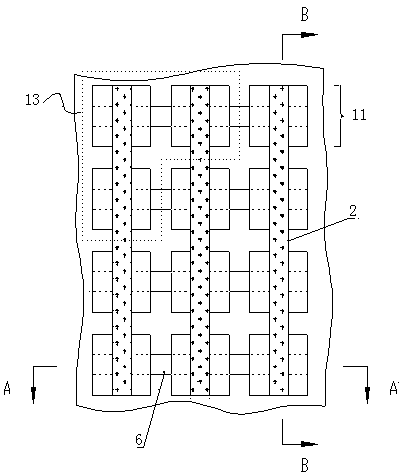
[0030] The micro light-emitting diode display of the present invention includes one or more display units, each display unit is composed of several pixels, and each pixel includes three or more sub-pixels, the pixels, sub-pixels in the present invention The pixels are made of III-V or II-VI semiconductor materials.

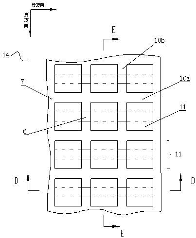
[0031] figure 1 It shows a partial top view of the same unit containing 3*4 sub-pixels. There is an etching gap between adjacent sub-pixels, and the sub-pixels 11 of the same column in a unit are connected to the same electrode A, and the electrode A is defined as One of the flexible N electrodes or flexible P electrodes, the sub-pixels in the same row in one unit are connected to the same electrode B, the electrode B is defined as the other of the flexible N electrodes or flexible P electrodes, and the flexible P electrodes As address scan electrodes, the flexible N electrodes are used as data drive electrodes to realize row and column drive. In this embodiment...


PUM


Abstract

The invention relates to a light emitting diode display structure. The display comprises one or more display units; and each display unit is composed of a plurality of pixels. The light emitting diodedisplay structure is characterized in that each pixel comprises three or more than three sub pixels; an etching gap exists between adjacent sub pixels; and sub pixels of the same column in one unit are connected to the same flexible electrode A, sub pixels of the same row in one unit are connected to the same flexible electrode B, and row-column driving is realized. The light emitting diode display structure has the advantages that the flexible light emitting diode display can be bent, a backlight source is not needed, and the display can be made thin; as the display is made by an inorganic semiconductor epitaxial wafer with stable performance, the service life is long, and a condition of uneven display does not happen; and the production process can be simplified to a great extent, and the production cost is reduced.

Description

technical field [0001] The invention relates to a display structure, in particular to a light emitting diode display structure. Background technique [0002] Displays are widely used in today's consumer electronics products, especially computer monitors, mobile phone displays, and smart wearable device displays. With the advancement of technology, the original cathode ray tube display has basically been replaced by the thin and light liquid crystal display (LCD), and is developing towards a lighter and thinner direction. The LCD itself does not emit light, and it needs a backlight to display normally, which limits the LCD from being thin enough. In recent years, organic light-emitting diode displays (OLEDs) have risen rapidly. With the advantages of self-illumination and no need for backlight sources, they can be made thinner and are widely used by some large companies in mobile phones, smart watches and other devices. [0003] And OLED also has its shortcomings that are d...

Claims


Application Information

Patent Timeline
Patent Type & Authority Applications(China)
IPC IPC(8): H01L27/15H01L33/36
CPCH01L27/15H01L33/36
Inventor 孙智江赵见国
Owner HAIDIKE NANTONG OPTOELECTRONICS TECH CO LTD
Why Eureka
Try Eureka