Inductor and printed circuit board with inductor

A printed circuit board and inductor technology, which is applied in the direction of printed circuits, printed circuits, and printed circuits connected with non-printed electrical components, and can solve problems such as unfavorable thinning of electronic products.

Inactive Publication Date: 2015-02-11
HONG FU JIN PRECISION IND WUHAN CO LTD +1
View PDF3 Cites 3 Cited by
  • Summary
  • Abstract
  • Description
  • Claims
  • Application Information

AI Technical Summary

Problems solved by technology

The conductive terminal of the existing chip inductor is under the inductor body. When the chip capacitor is mounted on a substrate, the thickness of the entire printed circuit board is...

Method used


Image

  • Inductor and printed circuit board with inductor
  • Inductor and printed circuit board with inductor
  • Inductor and printed circuit board with inductor

Examples


Embodiment Construction

[0013] Below in conjunction with accompanying drawing and preferred embodiment the present invention is described in further detail:

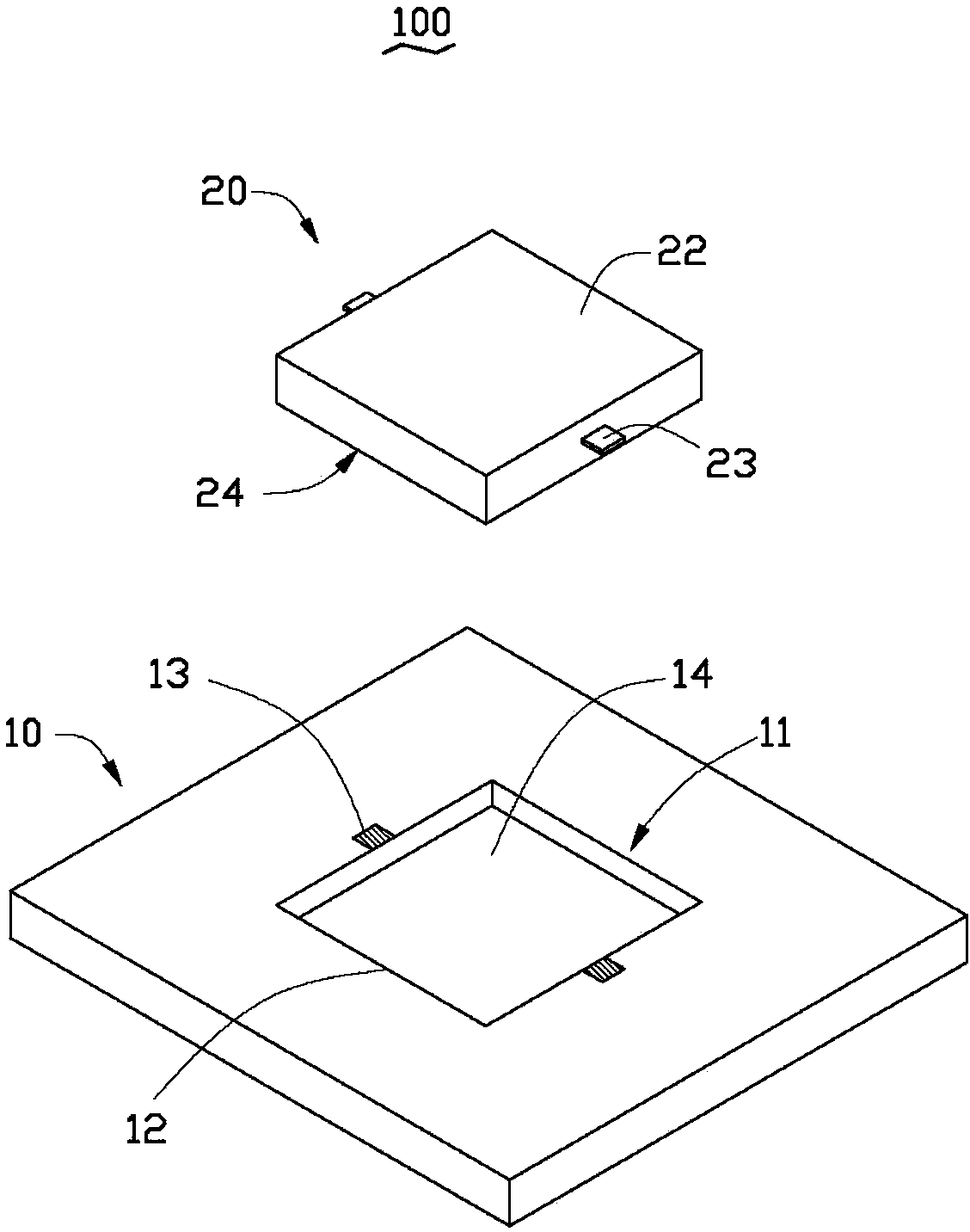
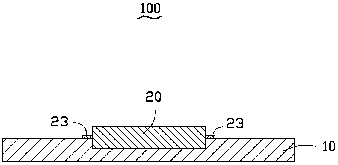
[0014] Please refer to figure 1 , the printed circuit board 100 of the present invention includes a substrate 10 and an inductor 20 disposed on the substrate 10 .

[0015] The inductor 20 includes a body 22 and two conductive terminals 23 disposed on the side of the body 22 . In this embodiment, the two conductive terminals 23 are respectively disposed on two opposite side surfaces of the body 22 .

[0016] The substrate 10 is provided with an installation area 11 for installing the inductor 20 , the installation area 11 includes an installation groove 12 and two pads 13 disposed around the installation groove 12 . In this embodiment, the two pads 13 are respectively disposed at two opposite ends of the installation groove 12 and correspond to the conductive terminals 23 . The installation slot 12 is used for installing the body 22 of the in...


PUM


Abstract

The invention relates to a printed circuit board, which comprises an inductor and a substrate, wherein the inductor is arranged on the substrate, and comprises a body and two conductive terminals, the two conductive terminals are arranged at the sides of the body, the substrate is provided with a mounting area for correspondingly mounting the inductor, the mounting area comprises a mounting groove and two welding pads, and the welding pads are arranged at the periphery of the mounting groove and correspond to the conductive terminals on the body. The printed circuit board has the advantage that the mounting groove for containing the inductor is arranged on the substrate, so the thickness of the printed circuit board is reduced, and the thinning of an electronic product is favorably realized.

Description

technical field [0001] The invention relates to an inductor and a printed circuit board installed with the inductor. Background technique [0002] With the development of science and technology, electronic products are developing towards light, thin, short, small and multi-functional integration. For inductors, flattening and miniaturization are also inevitable trends in their development. The conductive terminal of the existing chip inductor is under the inductor body. When the chip capacitor is mounted on a substrate, the thickness of the entire printed circuit board is the sum of the thickness of the capacitor body, the thickness of the conductive terminal of the capacitor, and the thickness of the substrate. , It is not conducive to making thin electronic products. Contents of the invention [0003] In view of the above, it is necessary to provide an inductor and a printed circuit board mounted with the inductor, so that the thickness of the printed circuit board can...

Claims


Application Information

Patent Timeline
IPC IPC(8): H05K1/18H05K1/02H05K1/11H01F27/29
CPCH05K1/111H01F27/292H05K1/183H05K2201/1003
Inventor 彭勃苏聪贤
Owner HONG FU JIN PRECISION IND WUHAN CO LTD
Why Eureka
Try Eureka