
Anti-interference design method applied to MCU reset system
A design method and high-level technology, applied in data reset devices, pulse processing, electrical components, etc., can solve the problems of occupying a large chip area, unstable filtering delay, etc., to achieve the effect of improving stability and flexible application
- Summary
- Abstract
- Description
- Claims
- Application Information
AI Technical Summary
Problems solved by technology
Method used
Image

Examples
Embodiment Construction
[0019] The following will clearly and completely describe the technical solutions in the embodiments of the present invention with reference to the accompanying drawings in the embodiments of the present invention. Obviously, the described embodiments are only some, not all, embodiments of the present invention. Based on the embodiments of the present invention, all other embodiments obtained by persons of ordinary skill in the art without making creative efforts belong to the protection scope of the present invention.
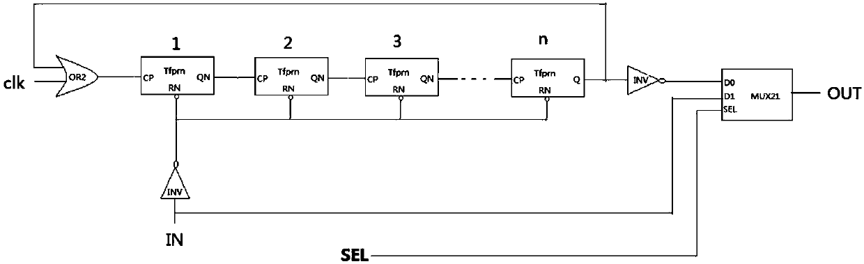
[0020] as follows figure 1 It is a schematic diagram of the logical structure of the anti-jamming design method. Among them, OR2: 2 input OR gate; Tfprn: T flip-flop triggered by rising edge and low level reset; INV: inverter; clk: input clock signal; MUX21: 2 to 1 data selector; SEL: data selection signal, SEL=0 selects D0, SEL=1 selects D1; IN: input signal; OUT: output signal;
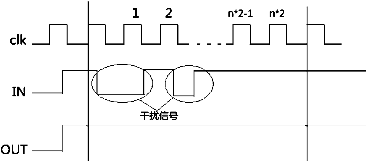
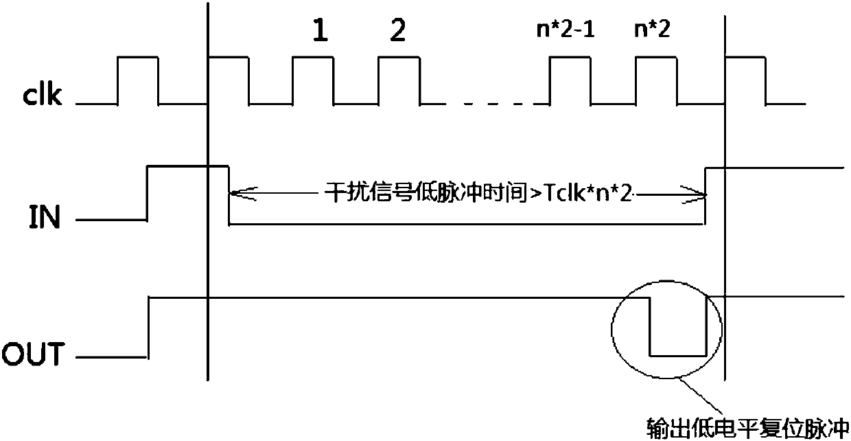
[0021] as follows figure 2 , SEL=0, signal transmission diagram (low-leve...
PUM
 Abstract
Description
Claims
Application Information