Display device and voltage compensation method thereof

A technology of display device and gamma voltage, applied in static indicators, instruments, etc., can solve the problems of increasing the power consumption of the display panel, avoid the problem of high power consumption, and improve the effect of brightness deviation

Active Publication Date: 2020-12-25
NANJING BOE DISPLAY TECH CO LTD
View PDF11 Cites 0 Cited by
  • Summary
  • Abstract
  • Description
  • Claims
  • Application Information

AI Technical Summary

Problems solved by technology

However, this compensation method needs to detect the feedback signal of the common voltage in the display panel all the time, and when the common voltage does not need to be compensated, the compensation circuit is always on, which will increase the power consumption of the display panel

Method used


Image

  • Display device and voltage compensation method thereof
  • Display device and voltage compensation method thereof
  • Display device and voltage compensation method thereof

Examples


Embodiment 1

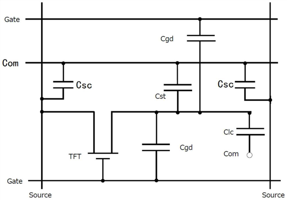
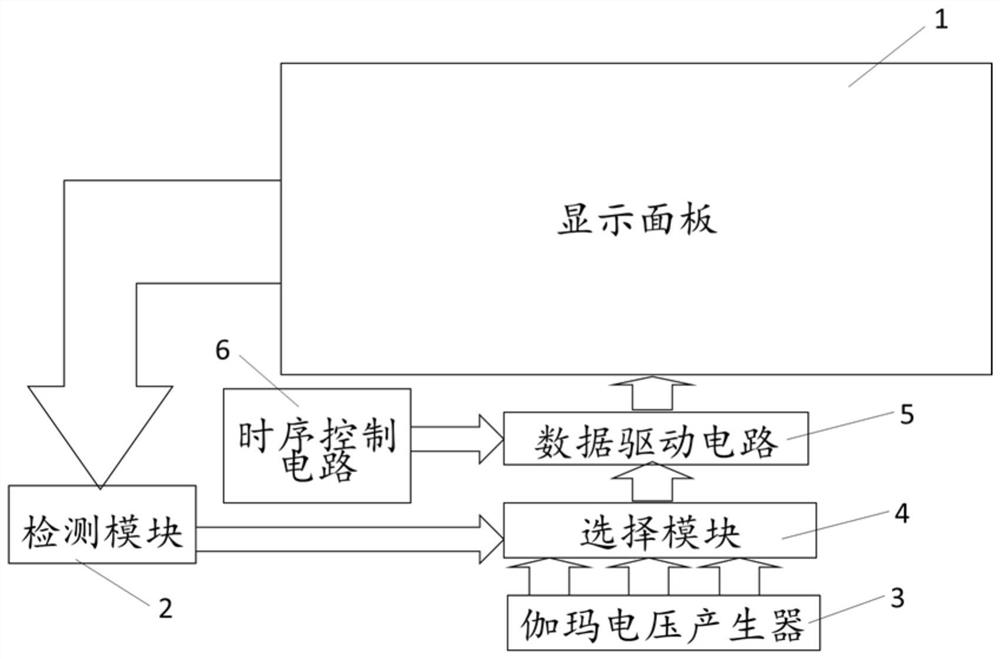
[0058] The structural schematic diagram of the display device in this embodiment is as follows figure 2 As shown, it includes a display panel 1 , a detection module 2 , a gamma voltage generator 3 , a selection module 4 , a data driving circuit 5 and a timing control circuit 6 . The display panel 1 has scanning lines and data lines criss-crossing, pixel areas defined by intersections of the scanning lines and data lines, and common electrode lines parallel to the scanning lines and formed on the same layer as the scanning lines.

[0059] In other embodiments, the common electrode lines can also be parallel to the data lines and formed simultaneously with the data lines; or the common electrode lines can also be parallel to the scanning lines and formed simultaneously with the data lines; or the common electrode lines can also be parallel to the scanning lines and The data lines are formed at the same time; or the common electrode lines are parallel to the scan lines and the d...

Embodiment 2

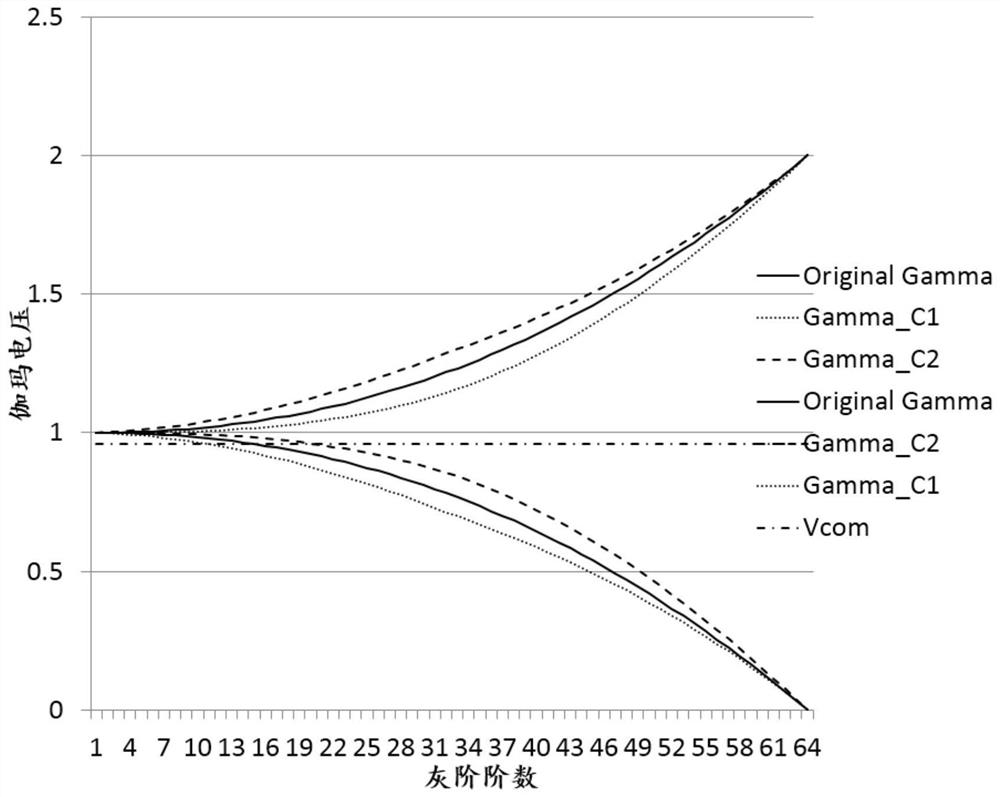
[0075] The structural schematic diagram of the display device in this embodiment is as follows Figure 4 shown. Different from Embodiment 1, the display device in this embodiment also includes a compensation module 7 and a DC filter 8. Since the selection module 4 selects one of the multiple gamma voltages according to the fluctuation of the common voltage, this selection is It is determined by the preset upper threshold and lower threshold, so this compensation is stepwise and not precise enough. The compensation module 4 can perform finer compensation on the selected gamma voltage, so that the voltage difference between the two ends of the liquid crystal is closer to the target voltage difference. The specific structure of the display device is as follows:

[0076] There are multiple detection points on the common electrode line, the detection module 2 is connected to the common electrode line and obtains the common voltage at the detection points, and inputs the common vol...

Embodiment 3

[0106] The structural schematic diagram of the display device in this embodiment is as follows Figure 9 shown. Different from Embodiment 1, this embodiment does not need to additionally set the selection module 4, but makes full use of the existing structure of the timing control circuit 6, and improves the existing look-up table 9 in the timing control circuit 6; in addition, in this implementation The gamma voltage generator 3 only needs to output one gamma voltage, which simplifies the circuit and saves the cost.

[0107] The existing timing control circuit 6 is usually provided with a LUT (look up table lookup table). Since the light transmittance of the display panel is different for different colors, the lookup table 9 is used for different color layers (such as red, green, blue or red, green, and blue). The gamma curve of white) is corrected separately, so that the output gamma voltage value corresponds to the actual transmittance of each gray scale. The value of thi...


PUM


Abstract

The invention discloses a display device and a voltage compensation method thereof. The display device comprises: a display panel, a gamma voltage generator, a detection module, a selection module anda data driving circuit. The gamma voltage generator generates and outputs a plurality of gamma voltages for a certain target grayscale. Coordinate points, with the target grayscale as the horizontalcoordinate and the plurality of gamma voltages as vertical coordinates, are located on a plurality of gamma voltage curves with different gamma values. The selection module inputs a single gamma voltage into the data driving circuit based on the common voltage. The display device selects the gamma voltage according to common voltage fluctuation and generates a compensated data voltage after processing by the data driving circuit, so that the fluctuation of the voltage difference between the two ends of the liquid crystal is reduced, thereby improving the deviation of brightness caused by common voltage fluctuation.

Description

technical field [0001] The invention relates to the field of display technology, in particular to a display device and a voltage compensation method thereof. Background technique [0002] In an LCD panel, the brightness displayed by a pixel is determined by the voltage difference across the liquid crystal. Such as figure 1 As shown, one end of the liquid crystal is the common voltage, and usually the whole panel uses the same common voltage; the other end is the data voltage, which is charged by the data line Source when the thin film transistor is turned on. When the thin film transistor is turned off, the pixel unit mainly relies on the liquid crystal capacitor Clc and the storage capacitor Cst to maintain the voltage difference (these two capacitors are usually connected in parallel). In addition to the above two capacitances, in the display panel, there are parasitic capacitances between the data lines, scanning lines, etc., and the common voltage lines, such as: Cgd: ...

Claims


Application Information

Patent Timeline
Patent Type & Authority Patents(China)
IPC IPC(8): G09G3/36
CPCG09G3/3696
Inventor 曾海博
Owner NANJING BOE DISPLAY TECH CO LTD
Why Eureka
Try Eureka