Method for etching one part of side wall to improve white pixel

A white pixel and sidewall technology, applied in electrical components, semiconductor/solid-state device manufacturing, circuits, etc., can solve the problems of easy leakage current and great impact on device performance, and achieve the goal of improving white pixels and reducing etching damage. Effect

Inactive Publication Date: 2018-04-13
SHANGHAI HUALI MICROELECTRONICS CORP
View PDF2 Cites 0 Cited by
  • Summary
  • Abstract
  • Description
  • Claims
  • Application Information

AI Technical Summary

Problems solved by technology

[0003] In the current manufacturing process of 55nm UTS (Ultra Thin Stack) image sensor, which is an ultra-thin stack image sensor, the etching step has a great influence on the performance of the device.
The damage caused by the etching process will lead to defects, which will easily generate leakage current and eventually form white pixels (white pixels are color pixels with faults on the screen), which will affect the use

Method used


Image

  • Method for etching one part of side wall to improve white pixel
  • Method for etching one part of side wall to improve white pixel
  • Method for etching one part of side wall to improve white pixel

Examples


Embodiment Construction

[0024] The present invention will be further described below in conjunction with the accompanying drawings and specific embodiments, but not as a limitation of the present invention.

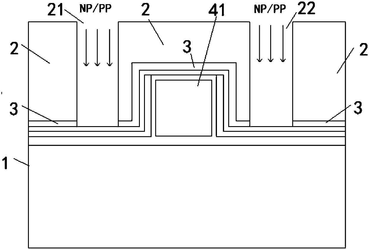
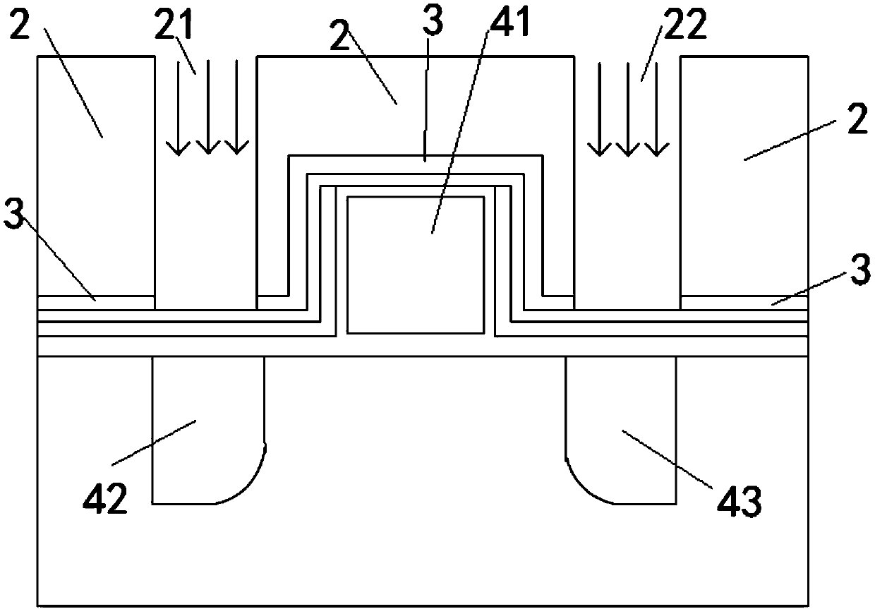
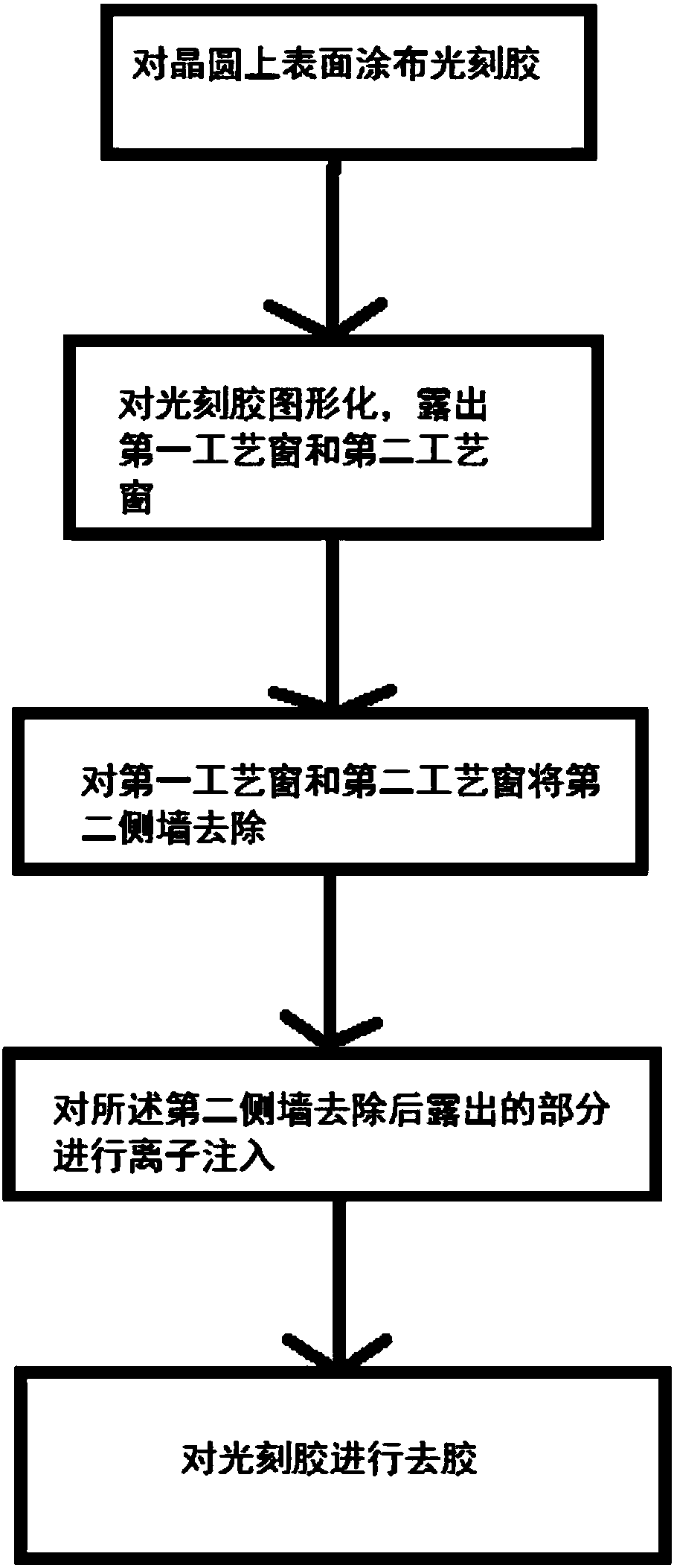
[0025] figure 1 is a schematic diagram of Step 3 of a method for improving white pixels by partial sidewall etching of the present invention; figure 2 is a schematic diagram of Step 4 of a method for improving white pixels by partial sidewall etching of the present invention; image 3 It is a flowchart of a method for improving white pixels by partial sidewall etching of the present invention.

[0026] The etching of the second sidewall 3 in the prior art is aimed at the entire wafer, but since there is no need to etch the other areas except the source 42 and the drain 43 , it needs to be reduced.

[0027] See Figure 1 to Figure 3 As shown, in a preferred embodiment, a method for improving white pixels by partial sidewall etching, including:

[0028] Step 1: Coating photoresist on the uppe...


PUM


Abstract

The invention discloses a method for etching one part of side wall to improve a white pixel. The method comprises the steps of (1) coating the upper surface of a wafer 1 with a photoresist; (2) patterning the photoresist and exposing a first process window and a second process window; (3) removing a second side wall through the first process window and the second process window; (4) carrying out ion implantation on the part exposed after the second side wall is removed; and (5) removing the photoresist. According to the method, etching of the second side wall is only carried out on the first process window and the second process window free of the photoresist, so that an unnecessary etching area is reduced, the etching damage is reduced and the white pixel is improved.

Description

technical field [0001] The invention relates to the technical field of integrated circuit manufacturing technology, in particular to the technical field of side wall etching. Background technique [0002] The existing stacked photosensitive element completely puts the circuit layer under the pixel layer, so that the amount of incoming light will be even greater, and the stacked type adds W to the three primary color pixels of R (red), G (green) and B (blue). (white) pixels, so that brighter photos can be taken in dark environments. [0003] However, in the manufacturing process of the current 55nm UTS (Ultra Thin Stack) image sensor, which is an ultra-thin stack image sensor, the etching step has a great influence on the performance of the device. The damage caused by the etching process will lead to defects, which will easily generate leakage current, and finally form white pixels (white pixels are color pixels that have failed on the screen), which will affect the use. ...

Claims


Application Information

Patent Timeline
IPC IPC(8): H01L21/027H01L21/265H01L21/3065
Inventor 孙赛俞敏曹亚民
Owner SHANGHAI HUALI MICROELECTRONICS CORP
Why Eureka
Try Eureka