Pulse combination femtosecond-nanosecond laser processing system and processing method

A femtosecond laser and laser processing technology, which is applied to laser welding equipment, metal processing equipment, manufacturing tools, etc., can solve problems such as limited use, low femtosecond laser pulse energy, and inability to significantly improve processing efficiency, achieving improved The effect of processing efficiency and ensuring accuracy

Active Publication Date: 2018-04-24
HARBIN INST OF TECH
View PDF7 Cites 11 Cited by
  • Summary
  • Abstract
  • Description
  • Claims
  • Application Information

AI Technical Summary

Problems solved by technology

However, due to the low pulse energy of the femtosecond laser, its processing efficiency cannot be significantly improved
Nanosecond lasers have the advantage

Method used


Image

  • Pulse combination femtosecond-nanosecond laser processing system and processing method
  • Pulse combination femtosecond-nanosecond laser processing system and processing method
  • Pulse combination femtosecond-nanosecond laser processing system and processing method

Examples


Embodiment 1

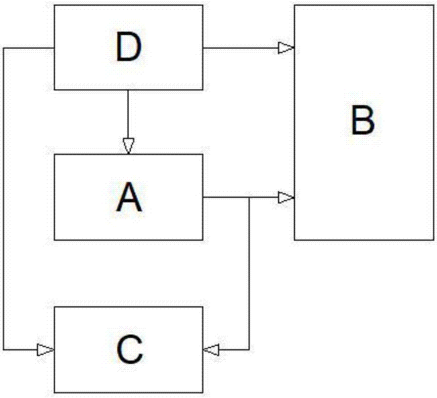
[0029] Such as figure 1As shown, a pulse-combined femtosecond-nanosecond laser processing system and processing method of the present invention include femtosecond-nanosecond double pulse laser system A, laser working system B, monitoring system C and power supply system D, femtosecond -Nanosecond double-pulse laser system A generates femtosecond-nanosecond double-pulse laser with pulse delay, and transmits it to laser working system B to process the workpiece. Monitoring system C is located between femtosecond-nanosecond double-pulse laser system A and Between the laser working system B, the monitoring system C is used to detect the actual pulse delay of the femtosecond-nanosecond double-pulse laser generated by the femtosecond-nanosecond double-pulse laser system A, and the power supply system D is the above-mentioned femtosecond-nanosecond double-pulse laser Power supply for laser system A, laser working system B, and monitoring system C.

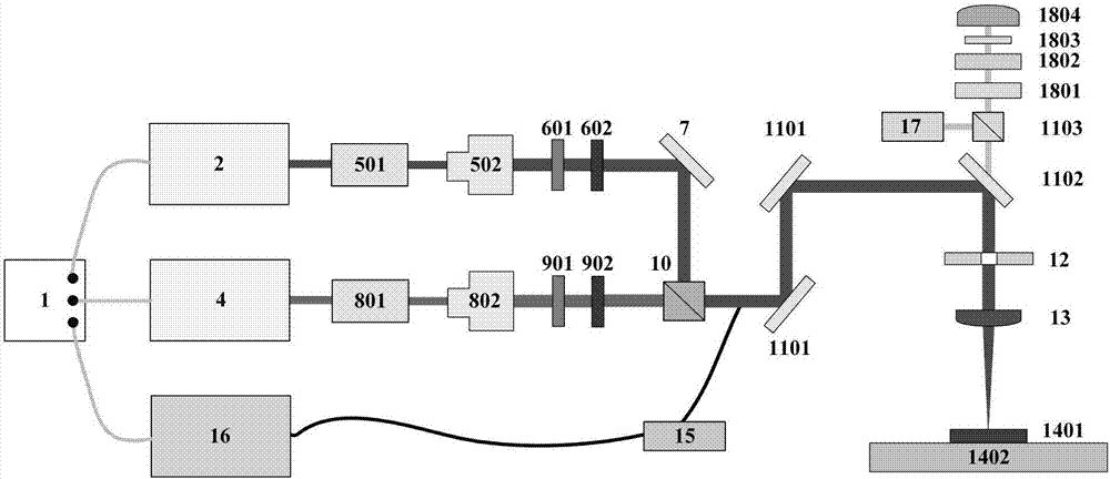
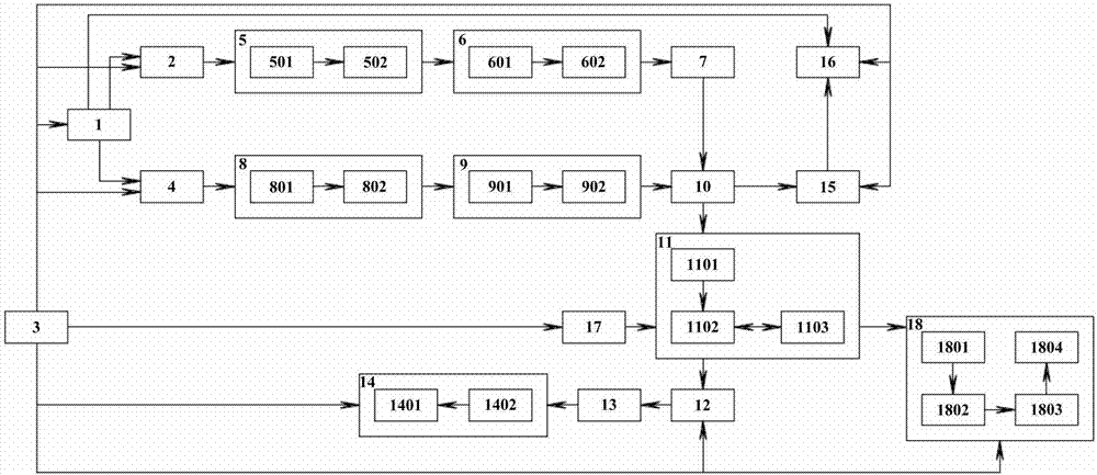
[0030] Such as figure 2 and 3...


PUM


Abstract

The present invention discloses a pulse combination femtosecond-nanosecond laser processing system and processing method. The system comprises a femtosecond-nanosecond dual-pulse laser system, a monitoring system, a laser working system and a power supply system. The femtosecond-nanosecond dual-pulse laser system generates femtosecond-nanosecond dual-pulse laser with pulse delay and transmits thefemtosecond-nanosecond dual-pulse laser to the laser working system to process workpieces. The monitoring system is positioned between the femtosecond-nanosecond dual-pulse laser system and the laserworking system to detect the real pulse delay of the femtosecond-nanosecond dual-pulse laser. The power supply system supplies all the above systems with power. Processing efficiency of semiconductormaterials is largely improved, the femtosecond-nanosecond dual-pulse laser waveform with a certain pulse delay, focusing conditions of laser spots, and processing processes can be observed in real time, and precision of the processing and processing quality of the semiconductor materials are ensured.

Description

technical field [0001] The invention relates to the application field of laser semiconductor processing, in particular to a pulse-combined femtosecond-nanosecond laser processing system and processing method. Background technique [0002] Semiconductor materials have good physical and chemical properties, such as corrosion resistance, small thermal expansion coefficient, and high hardness. Therefore, it is widely used in the fields of microelectronics, instrumentation and other fields. However, such materials are highly brittle, expensive, and require high processing quality during application. Common processing methods include grinding, reactive ion etching, and laser processing. The grinding cost of diamond grinding wheel is high, the reactive ion etching process is complex and the processing efficiency is low. At the same time, the semiconductor material has a large bandwidth and the absorption rate for short-pulse laser is very low. Therefore, although short-pulse lase...

Claims


Application Information

Patent Timeline
IPC IPC(8): B23K26/062
Inventor 杨立军丁烨程柏王懋露王扬
Owner HARBIN INST OF TECH
Why Eureka
Try Eureka