

Array substrate, display panel and display device
An array substrate and display area technology, which is applied in the fields of display panels, display devices, and array substrates, can solve problems such as poor display effects, and achieve the effects of improving display effects, improving packaging effects, and reducing stress.
- Summary
- Abstract
- Description
- Claims
- Application Information
AI Technical Summary
Problems solved by technology
Method used
Image

Examples
Embodiment Construction
[0023] In order to make the purpose, technical solution and advantages of the present invention clearer, the technical solution of the present invention will be fully described below through specific implementation in combination with the drawings in the embodiments of the present invention. Apparently, the described embodiments are some embodiments of the present invention, rather than all embodiments. Based on the embodiments of the present invention, all other embodiments obtained by persons of ordinary skill in the art without making creative efforts, All fall within the protection scope of the present invention.
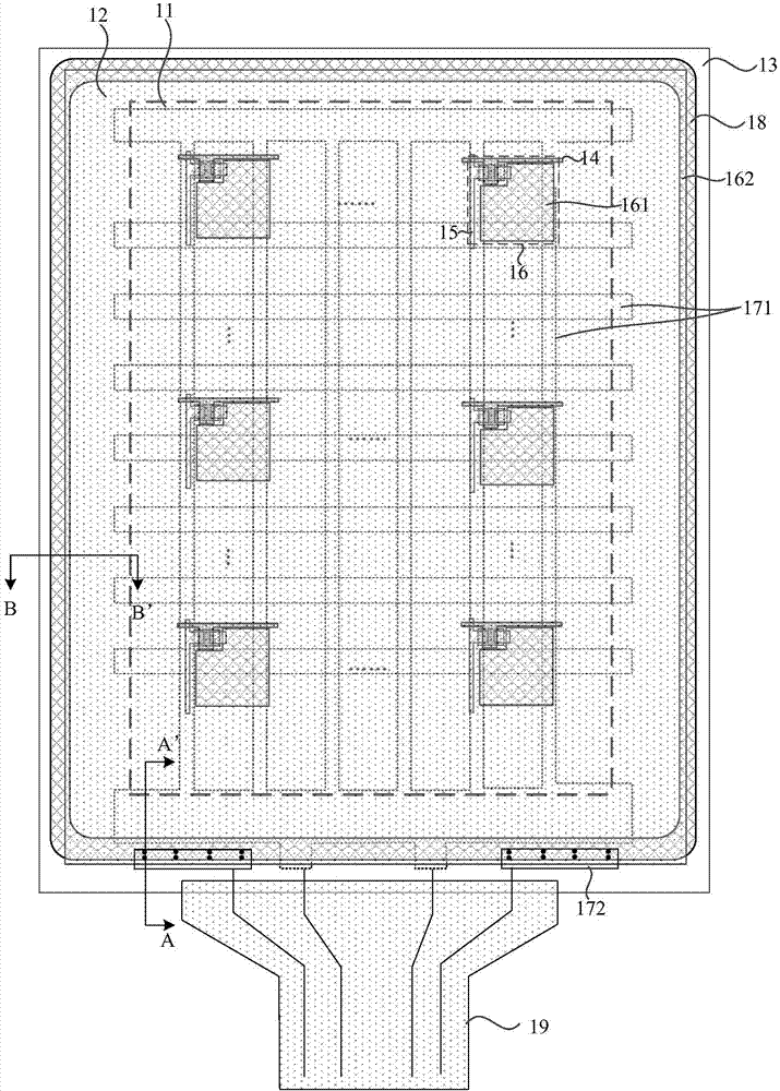
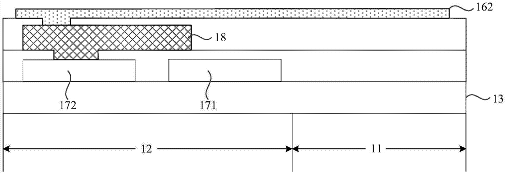
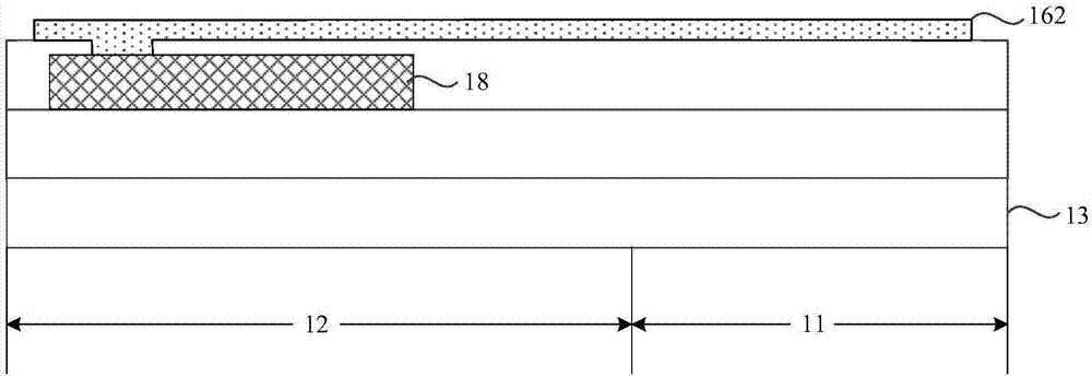
[0024] figure 1 is a structural schematic diagram of an array substrate in the prior art, figure 2 yes figure 1 The schematic diagram of the cross-sectional structure of the array substrate shown along the section line A-A' direction, image 3 yes figure 1 The schematic diagram of the cross-sectional structure of the array substrate along the section line B...
PUM
 Abstract
Description
Claims
Application Information