Design method for preventing negative voltage output of PSD signal processing circuit
A technology of signal processing circuit and design method, which is applied in the field of signal processing, and can solve problems such as damage to post-stage acquisition equipment, increased circuit complexity, and reduced reliability.
- Summary
- Abstract
- Description
- Claims
- Application Information
AI Technical Summary
Problems solved by technology
Method used
Image

Examples
Embodiment Construction
[0017] The present invention will be described in detail below in conjunction with specific embodiments. The following examples will help those skilled in the art to further understand the present invention, but do not limit the present invention in any form. It should be noted that those skilled in the art can make several changes and improvements without departing from the concept of the present invention. These all belong to the protection scope of the present invention.
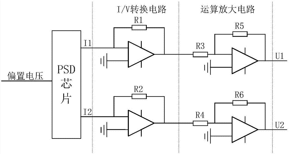
[0018] The pre-processing of the PSD signal generally uses a combination of an I / V conversion circuit and an operational amplifier circuit to convert the weak current signal output by the PSD device into a predetermined voltage signal for further acquisition and processing. Due to the inherent offset voltage and improper parameter design of the operational amplifier chip used in the I / V conversion circuit and operational amplifier circuit, the PSD signal processing circuit may output a negative voltage, ...
PUM
 Abstract
Description
Claims
Application Information
 - R&D
- Intellectual Property
- Life Sciences
- Materials
- Tech Scout
- Unparalleled Data Quality
- Higher Quality Content
- 60% Fewer Hallucinations
Browse by: Latest US Patents, China's latest patents, Technical Efficacy Thesaurus, Application Domain, Technology Topic, Popular Technical Reports.
© 2025 PatSnap. All rights reserved.Legal|Privacy policy|Modern Slavery Act Transparency Statement|Sitemap|About US| Contact US: help@patsnap.com