Solid-state image sensing device

a sensing device and solid-state technology, applied in the direction of radio frequency controlled devices, instruments, color signal processing circuits, etc., can solve the problems of difficult to divide the signal into signals, difficult to improve image quality, and non-uniformity in the dark

Active Publication Date: 2008-09-11
KK TOSHIBA
View PDF4 Cites 34 Cited by
  • Summary
  • Abstract
  • Description
  • Claims
  • Application Information

AI Technical Summary

Benefits of technology

[0006]According to an aspect of the invention, there is provided a solid-state image sensing device comprising: a pixel section in which cells are two-dimensionally arrayed in rows and columns on a semiconductor substrate, each cell including a photoelectric conversion unit, a reading circuit which reads out, to a detection unit, signal charges obtained by photoelectrically converting incident light by the photoelectric conversion unit, an amplifying circuit which amplifies and outputs a voltage corresponding to the signal charges stored in the detection unit, and a reset circuit which resets the signal charges of the detection unit; an exposure time control ci

Problems solved by technology

However, with this method an afterimage or white spot may form, and it is difficult to improve the image quality.
However, the dynamic range is widened using a detector, so no

Method used


Image

  • Solid-state image sensing device
  • Solid-state image sensing device
  • Solid-state image sensing device

Examples


first embodiment

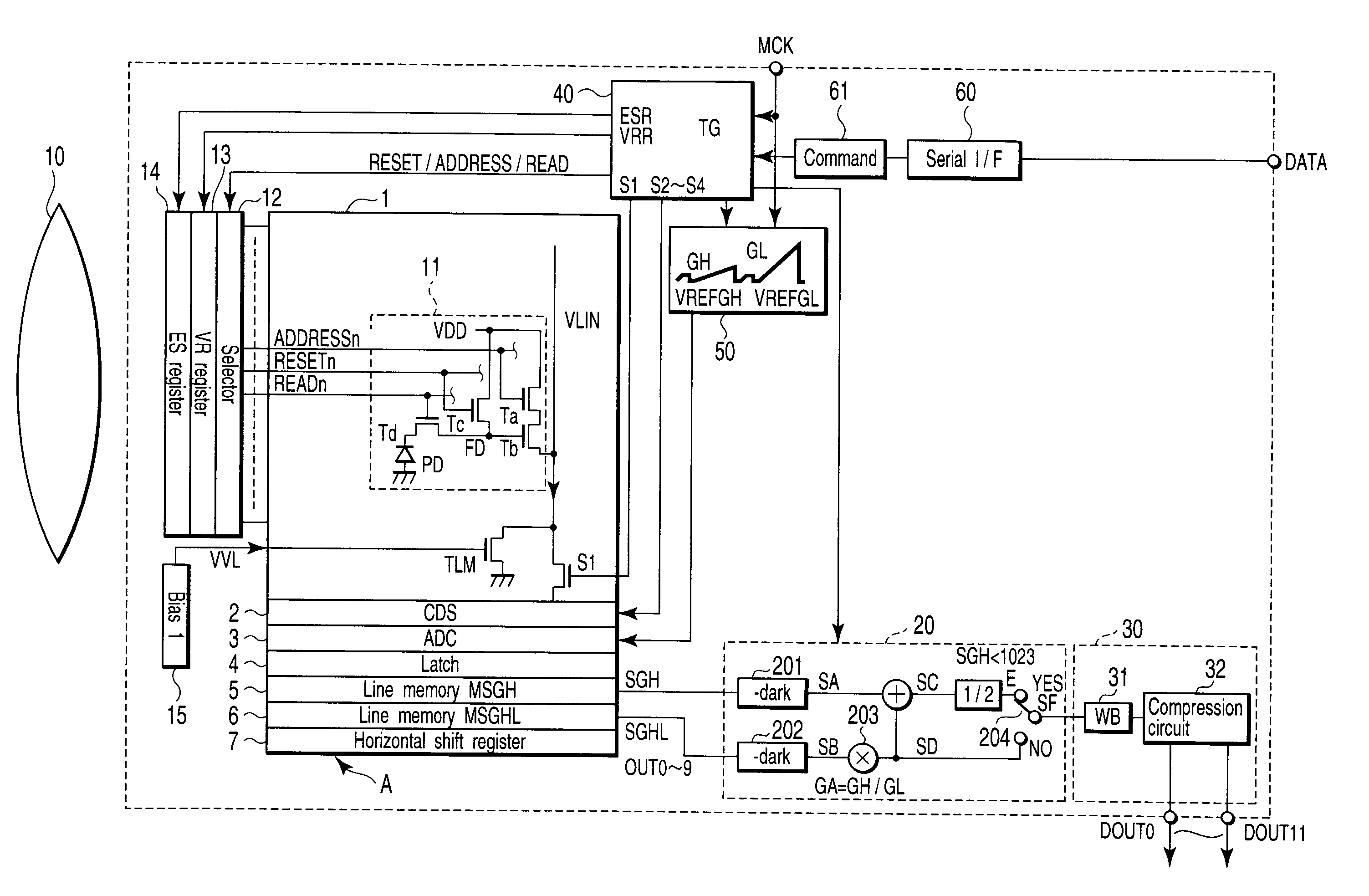
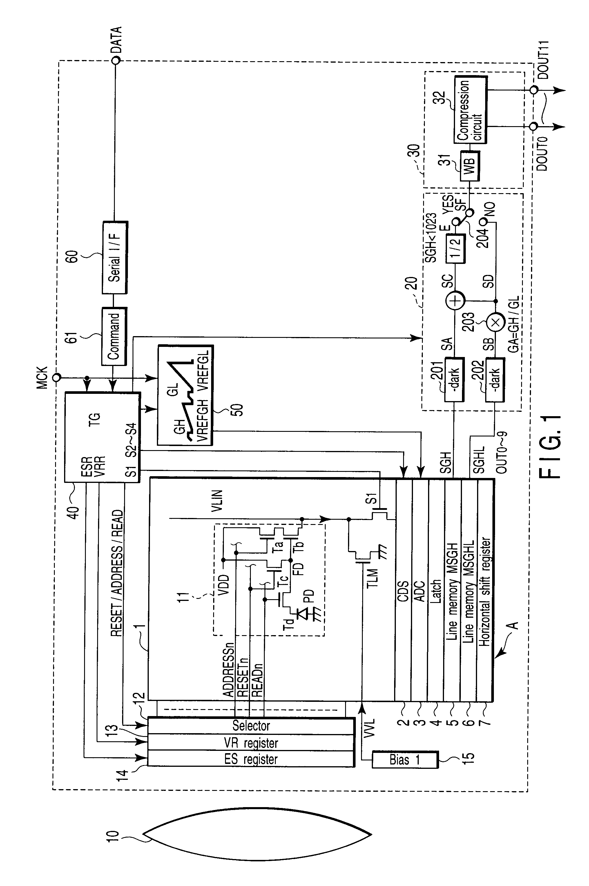
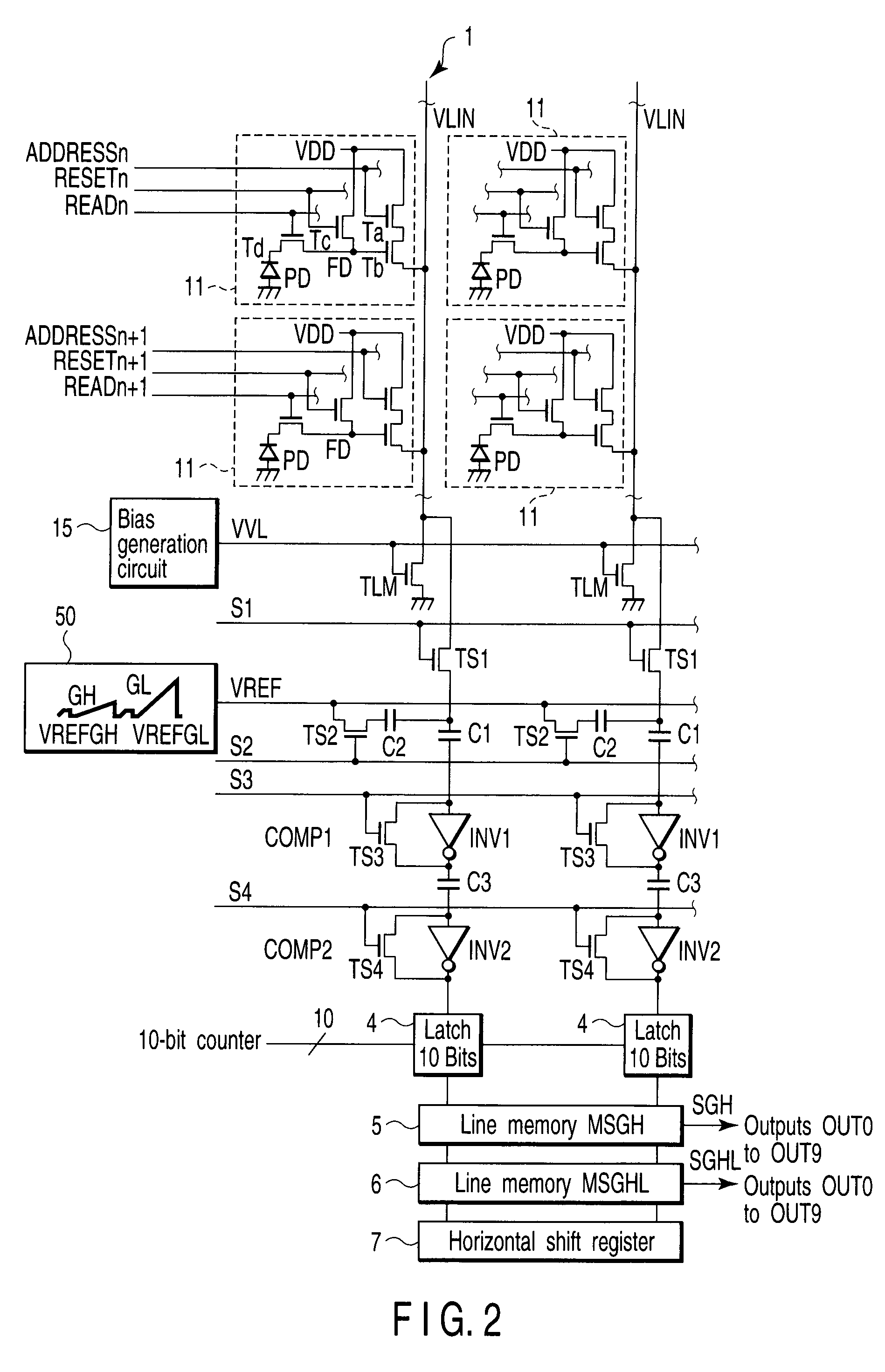
[0046]FIG. 1 is a block diagram showing the schematic arrangement of an amplifier type CMOS image sensor in order to explain a method of widening the dynamic range at low illuminance according to the present invention. A sensor core A comprises a pixel section 1, a column type noise canceling circuit (CDS) 2, a column type analog-to-digital converter (ADC) 3, a latch circuit 4, two line memories (MSGH and MSGHL) 5 and 6, and a horizontal shift register 7.

[0047]The pixel section 1 receives light via a lens 10, and generates charges corresponding to the incident light quantity by photoelectric conversion. In the pixel section 1, cells (pixels) 11 are two-dimensionally arrayed in rows and columns on a semiconductor substrate. One cell 11 has four transistors Ta, Tb, Tc, and Td and a photodiode PD. Each cell 11 receives pulse signals ADDRESSn, RESETn, and READn. Underneath the pixel section 1, load transistors TLM for a source follower circuit are arranged along the horizontal direction...

second embodiment

[0074]FIG. 8 is a block diagram showing the schematic arrangement of an amplifier type CMOS image sensor in order to explain a method of widening the dynamic range at low illuminance according to the present invention. In FIG. 8, the same reference numerals as those in FIG. 1 denote the same parts.

[0075]In FIG. 8, unlike FIG. 1, the former VREF amplitude of a VREF circuit 50 is set to the same gradient GL as that of the latter one. In a sensor core A, a column amplifier AMP 16 is interposed between a vertical signal line VLIN and a switch S1. The GAIN is multiplied by four in the first half of the horizontal scan period, and by one in the second half. This arrangement can reduce the noise mixing amount after the switch S1 to 1 / GAIN. The column amplifier AMP 16 may be an inverter AMP for the source follower. The column amplifier AMP 16 may be of an inversion type. In this case, for example, the waveform VREF needs to be inverted. A timing generator 40 supplies a signal to a pulse amp...

third embodiment

[0078]FIG. 11 is a block diagram showing the schematic arrangement of an amplifier type CMOS image sensor in order to explain a method of widening the dynamic range at low illuminance according to the present invention. In FIG. 11, the same reference numerals as those in FIG. 1 denote the same parts.

[0079]In FIG. 11, unlike FIG. 1, the latter VREFGL waveform of a VREF circuit 50 is set to the same gradient GH as that of VREFGH. A signal obtained by VREFGL is stored in a line memory MSGHL 6, and output as a signal SGHL from a sensor core A. A WDM circuit 20 adds signals SA and SB from which the black level (dark) is simply subtracted, and halves the signal level. Thus, the number of bits does not increase, and the signal SF becomes a 10-bit signal. Further, similar to FIG. 1, random noise can be reduced by 3 dB. If the WDM circuit 20 does not halve the signal level, an 11-bit signal SF is generated. The signal read timing is as shown in FIG. 3 or 4.


PUM


Abstract

There is provided a solid-state image sensing device including a pixel section in which cells are arrayed, each cell including a photoelectric conversion unit, a reading circuit reading out, to a detection unit, signal charges obtained by the photoelectric conversion unit, an amplifying circuit amplifying and outputting a voltage corresponding to the signal charges, and a reset circuit resetting the signal charges, an exposure time control circuit controlling an exposure time and controlling the exposure time to be equal for all cells, an A/D conversion circuit A/D-converting a signal output from the pixel section by changing a resolution of a signal level, line memories storing an A/D-converted signal, and a signal processing circuit processing output signals from the line memories to have a linear gradient with respect to an optical input signal amount by controlling an amplification factor in accordance with a resolution of a pixel output signal after A/D-conversion.

Description

CROSS-REFERENCE TO RELATED APPLICATIONS[0001]This application is based upon and claims the benefit of priority from prior Japanese Patent Application No. 2006-307257, filed Nov. 13, 2006, the entire contents of which are incorporated herein by reference.BACKGROUND OF THE INVENTION[0002]1. Field of the Invention[0003]The present invention relates to a solid-state image sensing device and, more particularly, to a CMOS image sensor used in a cell phone, digital camera, or video camera equipped with an image sensor.[0004]2. Description of the Related Art[0005]A conventional method of widening the dynamic range of a CMOS image sensor is described in, e.g., Jpn. Pat. Appln. KOKAI Publication Nos. 2001-189893 and 2000-23044. In Jpn. Pat. Appln. KOKAI Publication No. 2001-189893, the method of widening the dynamic range is applied to an incomplete transfer type photodiode. However, with this method an afterimage or white spot may form, and it is difficult to improve the image quality. To th...

Claims


Application Information

Patent Timeline
IPC IPC(8): H04N5/335H01L27/146H04N5/353H04N5/355H04N5/369H04N5/374H04N5/3745H04N5/376H04N5/378
CPCH01L27/14643H04N5/243H04N5/378H04N5/3745H04N5/35527H04N23/76H04N25/575H04N25/583H04N25/77H04N25/75
Inventor EGAWA, YOSHITAKA
Owner KK TOSHIBA
Why Eureka
Try Eureka