Display panel and manufacturing method thereof

A technology of display panel and manufacturing method, applied in semiconductor/solid-state device manufacturing, electrical components, electrical solid-state devices, etc., can solve problems such as limiting display quality, large cathode impedance, reducing current conduction capability, etc., so as to improve display quality, reduce Impedance, the effect of improving electron injection efficiency

Inactive Publication Date: 2018-05-11
TCL CHINA STAR OPTOELECTRONICS TECH CO LTD
View PDF3 Cites 5 Cited by
  • Summary
  • Abstract
  • Description
  • Claims
  • Application Information

AI Technical Summary

Problems solved by technology

When the thickness of the cathode is small, the cathode has a large impedance, which is not conducive to electron injection at this time, thereby reducing the conduction capacity of the current and limiting the improvement of the display quality

Method used


Image

  • Display panel and manufacturing method thereof
  • Display panel and manufacturing method thereof
  • Display panel and manufacturing method thereof

Examples


Embodiment Construction

[0024] The word "embodiment" as used in this specification means an example, instance or illustration. Furthermore, as used in this specification and the appended claims, the article "a" or "an" may generally be construed as "one or more" unless specified otherwise or clear from the context in the singular.

[0025] The display panel of the present invention is an OLED (Organic Light Emitting Diode, organic light emitting diode display panel) or the like.

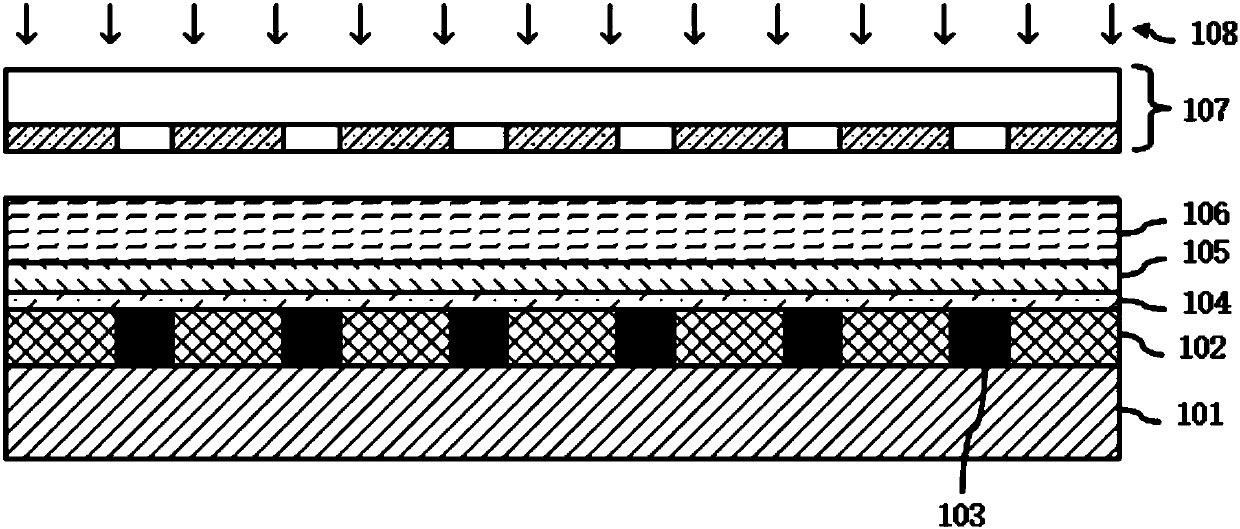
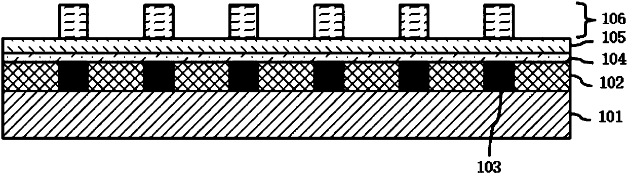
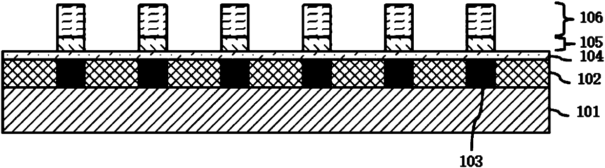
[0026] refer to Figure 5 , Figure 5 It is a schematic diagram of a partial section of the display panel of the present invention.

[0027] The display panel of the present invention includes a thin film transistor array substrate 101 , an organic light emitting functional layer, a pixel defining layer, a cathode layer, and a transparent encapsulation layer 501 .

[0028] The thin film transistor array substrate 101 includes a thin film transistor switch array and an anode array, the thin film transistor switches in the...


PUM


Abstract

The invention discloses a display panel and a manufacturing method thereof. The display panel comprises a thin film transistor array substrate, an organic light emitting functional layer, a pixel definition layer, a negative electrode layer and a transparent packaging layer; pixel definition components of the pixel definition layer are arranged on at least one side of the part, corresponding to the pixel unit of the display panel, in the organic light emitting functional layer; the negative electrode layer has predetermined light transmittance; the negative electrode layer covers the organic light emitting functional layer and the pixel definition layer; the thickness of the part, corresponding to an opening region of the display panel, of the negative electrode layer is less than the thickness of the part, corresponding to a non-opening region of the display panel, of the negative electrode layer; and the transparent packaging layer covers a conductive metal film layer and a conductive metal component layer, wherein the display panel is used for outputting a displayed image on the outer surface of the transparent packaging layer. By virtue of the display panel and the manufacturing method thereof, the electron injection efficiency of the display panel can be improved, and the display quality of the display panel can be further improved.

Description

【Technical field】 [0001] The invention relates to the field of display technology, in particular to a display panel and a manufacturing method thereof. 【Background technique】 [0002] Traditional OLED panels are generally bottom-emitting display panels, that is to say, traditional OLED panels generally output display images on the side corresponding to the anode layer. [0003] The drive circuit in the traditional OLED panel occupies a large area of ​​the pixel unit, therefore, the aperture ratio of the pixel unit is low, which leads to the unsatisfactory display effect of the traditional OLED panel. [0004] In order to solve the above-mentioned technical problems, an improvement solution is to change the traditional OLED panel into a top-light display panel, that is, to output a display image on the side of the OLED panel corresponding to the encapsulation layer. This improvement greatly increases the aperture ratio. [0005] However, in the above improvement scheme, the...

Claims


Application Information

Patent Timeline
Patent Type & Authority Applications(China)
IPC IPC(8): H01L27/32H01L51/52H01L51/56
CPCH10K59/12H10K50/82H10K71/00
Inventor 徐向阳
Owner TCL CHINA STAR OPTOELECTRONICS TECH CO LTD
Why Eureka
Try Eureka