Structure of flash memory and its operation method

An operation method and technology of flash memory, applied in the direction of electrical components, electric solid-state devices, circuits, etc., can solve the problems of low programming speed, asymmetric programming of memory cells, and low programming current, so as to reduce the current of memory cells and avoid Programming asymmetry, the effect of improving the operation speed

Inactive Publication Date: 2006-06-14
POWERCHIP SEMICON CORP
View PDF0 Cites 0 Cited by
  • Summary
  • Abstract
  • Description
  • Claims
  • Application Information

AI Technical Summary

Problems solved by technology

[0008] In the programming method of the above-mentioned double flash memory cell, after the memory cell 101a is programmed, when the memory cell 101b is programmed again, because the memory cell 101b will be affected by the programmed memory cell 101a, the programming current will change. Low, so the programming speed of memory cell 101b will be slower than that of memory cell 101a
This will cause the problem of memory cell programming asymmetry, resulting in slower memory cell operation speed.

Method used


Image

  • Structure of flash memory and its operation method
  • Structure of flash memory and its operation method
  • Structure of flash memory and its operation method

Examples


Embodiment Construction

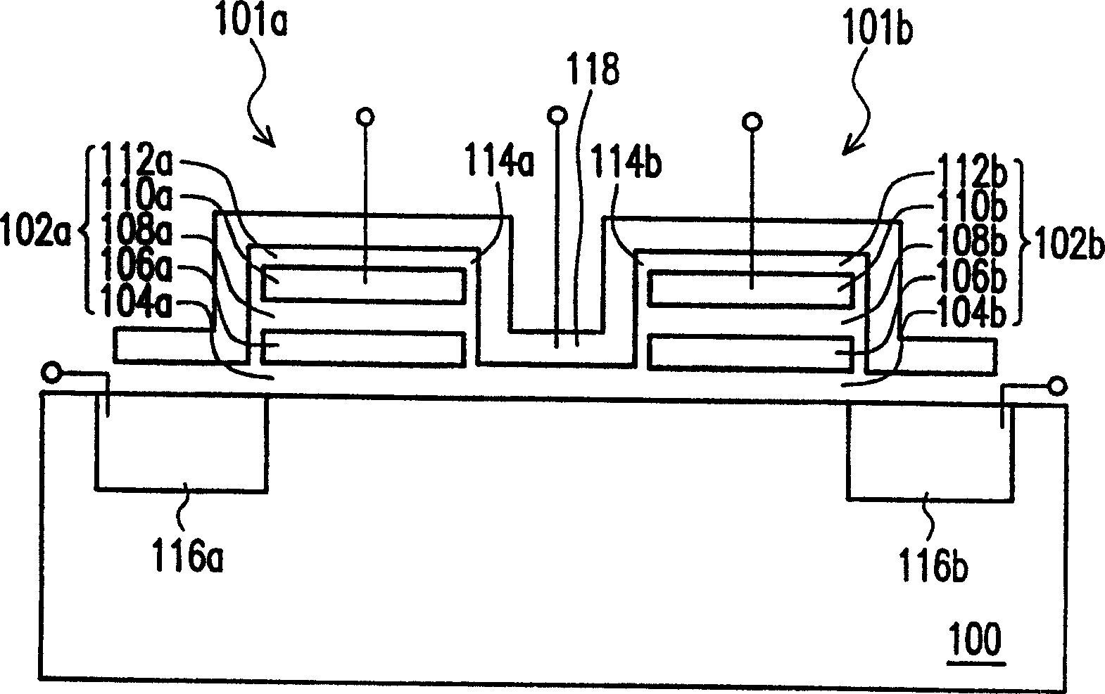
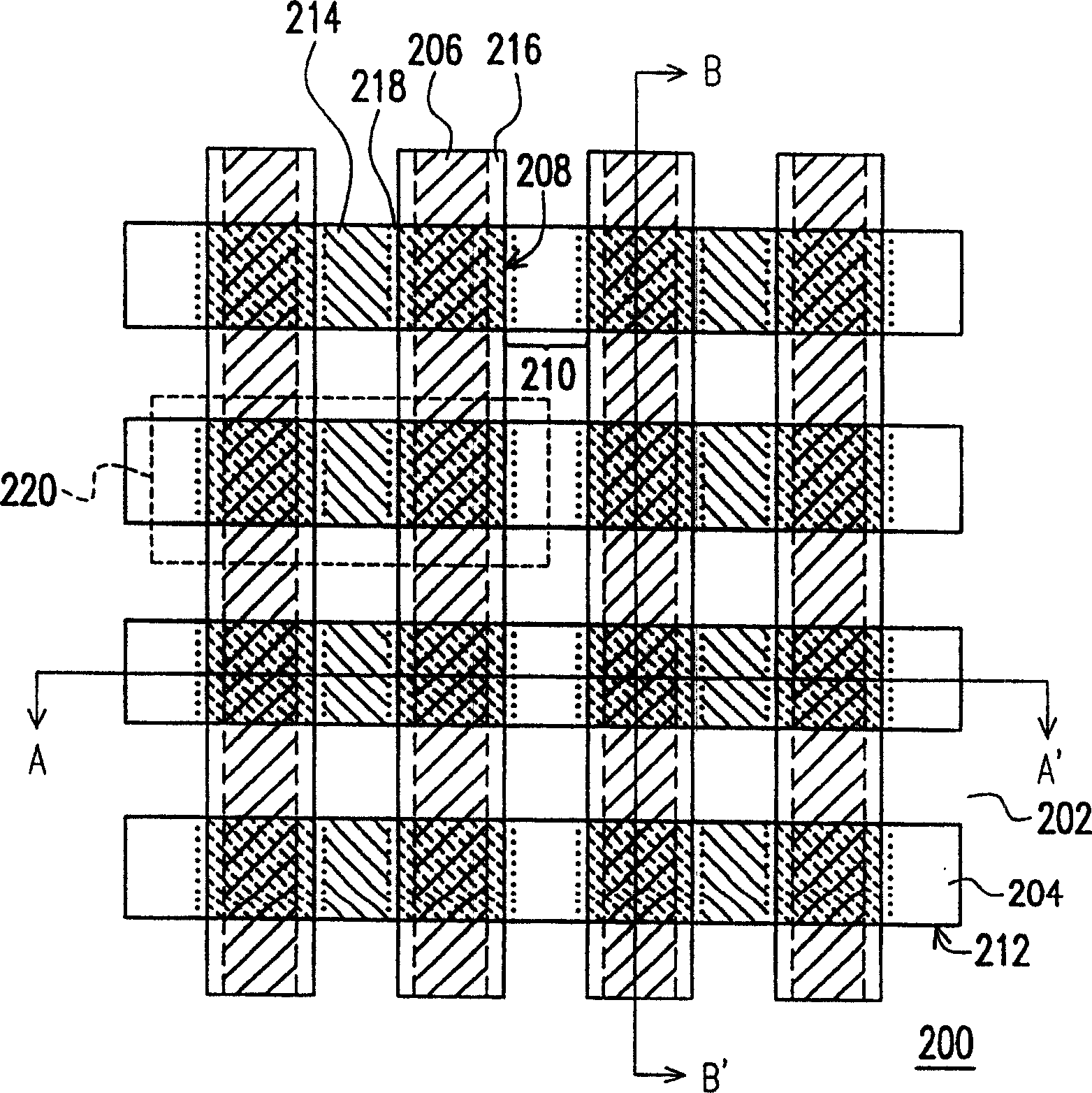
[0052] figure 2 It is a top view of the flash memory of the present invention. Please refer to figure 2 The flash memory of the present invention is composed of a substrate 200, an element isolation structure 202, an active region 204, a control gate 206 (word line), a floating gate 208, an N-type source / drain region 210, and a P-type well region 312 with select gate 214. constituted. Wherein, an insulating layer (spacer) 216 and an insulating layer (spacer) 218 ​​are disposed between the select gate 214 , the control gate 206 , and the floating gate 208 . A deep N-type well region (not shown) is disposed in the substrate 200 , and a P-type well region 212 is disposed on the deep N-type well region. The device isolation structure 202 is disposed in the substrate 200 to define the active region 204 so that the P-type well region 212 is only located in the active region 204 . The control gate 206 is disposed on the substrate 200 and perpendicular to the active region 204 ...


PUM


Abstract

A structure of flash memory, the structure of the flash memory element is composed of a P-type substrate, a deep N-type well region arranged in the P-type substrate, a P-type well region arranged in the deep N-type well region, and a P-type well region arranged on the P-type substrate A pair of gate structures, a selection gate disposed between the pair of gate structures, and an N-type source / drain region disposed in the P-type well region on both sides of the pair of gate structures. Since every two adjacent two-gate structures share one select gate, the integration of elements can be increased.

Description

technical field [0001] The present invention relates to a memory device, and in particular to a flash memory structure and its operating method. Background technique [0002] Flash memory elements have the advantages of being able to store, read, and erase data multiple times, and the stored data will not disappear after power failure, so it has become a widely used device in personal computers and electronic devices. A non-volatile memory element. [0003] A typical flash memory device uses doped polysilicon to make a floating gate (Floating Gate) and a control gate (Control Gate). Moreover, the control gate is directly arranged on the floating gate, the floating gate and the control gate are separated by a dielectric layer, and the floating gate and the substrate are separated by a tunnel oxide (Tunnel Oxide) ( Also known as stacked gate flash memory). [0004] When writing data into the flash memory, a bias voltage is applied to the control gate and the source / drain re...

Claims


Application Information

Patent Timeline
Patent Type & Authority Patents(China)
IPC IPC(8): H01L27/112H01L27/105H01L21/8246
Inventor 洪至伟宋达许正源
Owner POWERCHIP SEMICON CORP
Why Eureka
Try Eureka