Semiconductor device

a technology of semiconductor devices and semiconductors, applied in semiconductor devices, electrical equipment, instruments, etc., can solve the problems of long time-consuming storage of data, achieve the effect of reducing power consumption, and ensuring the safety of data

Active Publication Date: 2011-06-30
SEMICON ENERGY LAB CO LTD
View PDF68 Cites 86 Cited by
  • Summary
  • Abstract
  • Description
  • Claims
  • Application Information

AI Technical Summary

Benefits of technology

[0020]One embodiment of the present invention provides a semiconductor device including a transistor using an oxide semiconductor. Since the off current of a transistor using an oxide semiconductor is extremely low, stored data can be stored for an extremely long time by using the transistor. In other words, power consumption can be considerably reduced because refresh operation becomes unnecessary or the frequency of refresh operation can be extremely low. Moreover, stored data can be stored for a long time even when power is not supplied.
[0021]Further, a semiconductor device according to one embodiment of the disclosed invention does not need high voltage for writing of data and there is no problem of deterioratio...

Problems solved by technology

A transistor formed using a highly purified oxide semiconductor has ex...

Method used


Image

  • Semiconductor device
  • Semiconductor device
  • Semiconductor device

Examples


embodiment 1

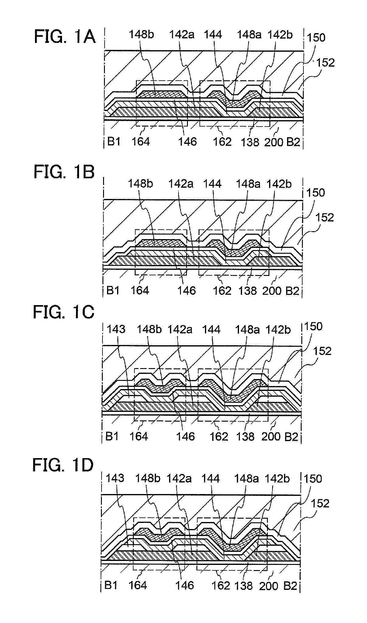
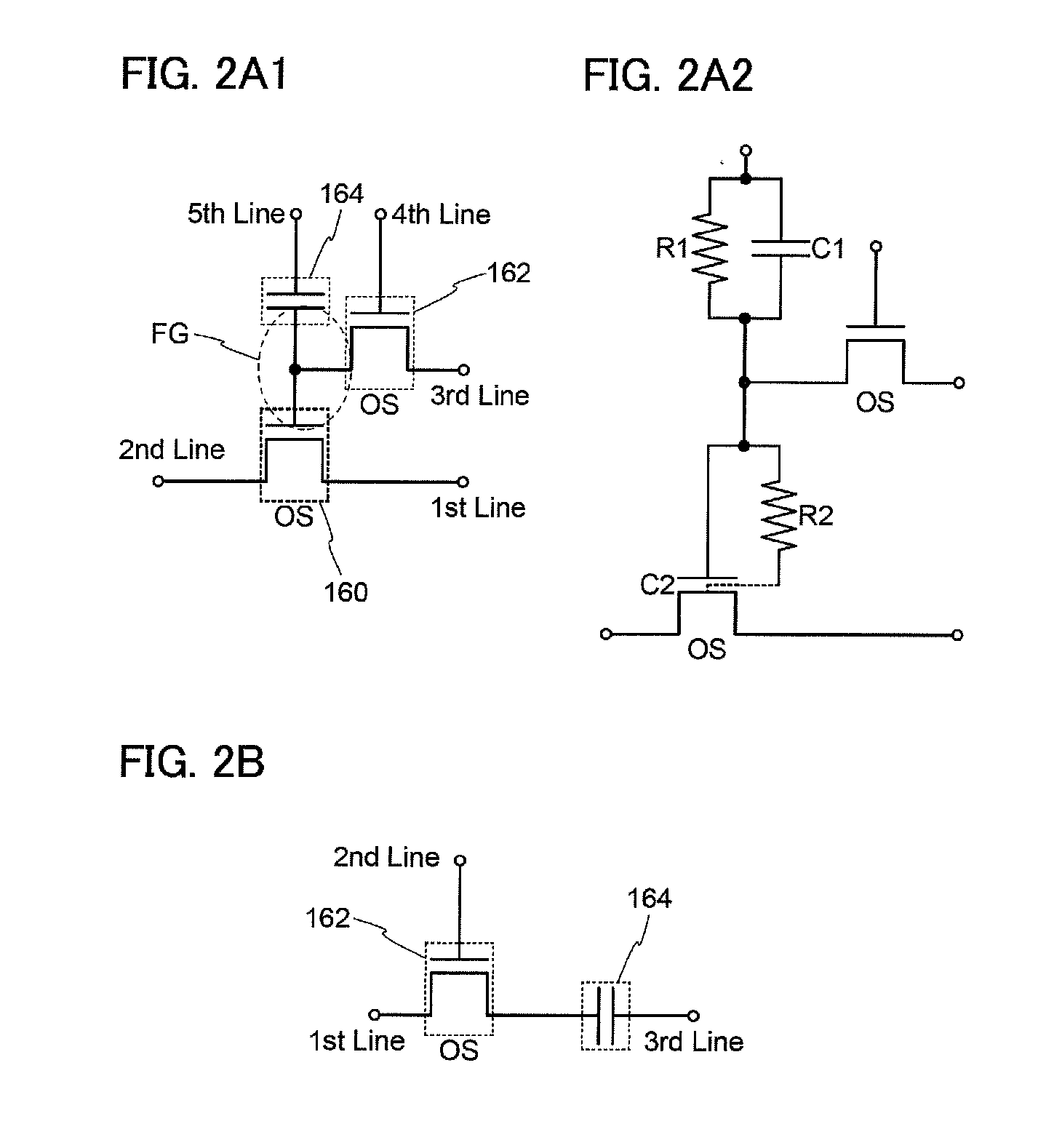
[0038]In this embodiment, structures and a manufacturing method of a semiconductor device according to one embodiment of the disclosed invention will be described with reference to FIGS. 1A to 1D and FIGS. 2A1, 2A2, and 2B. Note that in some of the circuit diagrams, “OS” is written beside a transistor in order to indicate that the transistor uses an oxide semiconductor.

[0039]FIGS. 1A to 1D each illustrate an example of a structure of the semiconductor device. FIGS. 1A to 1D each illustrate a cross section of the semiconductor device. The semiconductor devices illustrated in FIGS. 1A to 1D each include a transistor 162 using an oxide semiconductor and a capacitor 164.

[0040]Although all the transistors are described as n-channel transistors here, it is needless to say that p-channel transistors can be used. Since the technical nature of the disclosed invention is to use an oxide semiconductor in the transistor 162 so that data can be stored, it is not necessary to limit a specific str...

embodiment 2

[0083]In this embodiment, a manufacturing method of a semiconductor device using an oxide semiconductor, specifically a manufacturing method of the transistor 162, will be described with reference to FIGS. 3A to 3E.

[0084]First, the insulating layer 138 is formed over the substrate 200. After that, a conductive layer is formed over the insulating layer 138 and is selectively etched, so that the source or drain electrode 142a and the source or drain electrode 142b are formed (see FIG. 3A).

[0085]As the substrate 200, for example, a glass substrate can be used. Alternatively, as the substrate 200, as well as a glass substrate, an insulating substrate formed using an insulator such as a ceramic substrate, a quartz substrate, or a sapphire substrate, a semiconductor substrate formed using a semiconductor material such as silicon, a conductive substrate formed using a conductor such as metal or stainless steel, any of these substrate whose surface is covered with an insulating material, or...

embodiment 3

[0123]In this embodiment, a manufacturing method of a transistor using an oxide semiconductor (especially, an oxide semiconductor having an amorphous structure) will be described with reference to FIGS. 4A to 4E. The transistor can be used instead of the transistor 162 or the like in any of the above embodiments. A structure of the transistor according to this embodiment and the structure of the transistor according to any of the above embodiments are partly common to each other. Therefore, a difference is mainly described below. A top-gate transistor is described below as an example; however, a structure of the transistor is not limited to a top-gate structure.

[0124]First, an insulating layer 202 is formed over the substrate 200. After that, an oxide semiconductor layer 206 is formed over the insulating layer 202 (see FIG. 4A).

[0125]For example, the substrate 200 in any of the above embodiments can be used for the substrate 200 in this embodiment.

[0126]The insulating layer 202 corr...


PUM


Abstract

An object of the present invention is to provide a semiconductor device having a novel structure in which in a data storing time, stored data can be stored even when power is not supplied, and there is no limitation on the number of writing. A semiconductor device includes a first transistor including a first source electrode and a first drain electrode; a first channel formation region for which an oxide semiconductor material is used and to which the first source electrode and the first drain electrode are electrically connected; a first gate insulating layer over the first channel formation region; and a first gate electrode over the first gate insulating layer. One of the first source electrode and the first drain electrode of the first transistor and one electrode of a capacitor are electrically connected to each other.

Description

TECHNICAL FIELD[0001]The disclosed invention relates to a semiconductor device using a semiconductor element and a manufacturing method of the semiconductor device.BACKGROUND ART[0002]Memory devices using semiconductor elements are broadly classified into two categories: a volatile memory device that loses stored data when power supply stops, and a non-volatile memory device that stores stored data even when power is not supplied.[0003]A typical example of a volatile memory device is a DRAM (dynamic random access memory). A DRAM stores data in such a manner that a transistor included in a memory element is selected and charge is stored in a capacitor.[0004]When data is read from a DRAM, charge in a capacitor is lost on the above-described principle; thus, another writing operation is necessary whenever data is read out. Moreover, a transistor included in a memory element has leakage current and charge flows into or out of a capacitor even when the transistor is not selected, so that...

Claims


Application Information

Patent Timeline
IPC IPC(8): H01L27/108
CPCH01L27/1225H01L29/7869H01L27/11517H01L21/84H01L27/11H01L27/1108H01L27/1255G11C16/26H01L27/11521H01L27/1156G11C16/0433H01L27/11803H01L27/108H01L27/10873H10B12/00H10B12/05H10B10/125H10B10/00H10B41/00H10B41/30H10B41/70H01L29/24H10B12/30
Inventor YAMAZAKI, SHUNPEIKOYAMA, JUNKATO, KIYOSHI
Owner SEMICON ENERGY LAB CO LTD
Why Eureka
Try Eureka