Flash memory unit, flash memory unit array and mfg. method thereof

A memory cell array and memory cell technology, which is applied in semiconductor/solid-state device manufacturing, electrical components, electric solid-state devices, etc., can solve the problems of slow operation speed of memory cells, small reading current of memory cells, and inability to improve device performance, etc. , to achieve the effect of improving operation speed and performance, improving gate coupling rate, and high electron injection efficiency

Inactive Publication Date: 2007-05-23
POWERCHIP SEMICON CORP
View PDF2 Cites 0 Cited by
  • Summary
  • Abstract
  • Description
  • Claims
  • Application Information

AI Technical Summary

Problems solved by technology

However, the program of writing and reading the memory cells in the NAND array is relatively complicated, and because many memory cells are connected in series in the array, the read current of the memory cells is relatively small, and the A problem that causes the operation speed of the memory cell to slow down, and the performance of the device cannot be improved

Method used


Image

  • Flash memory unit, flash memory unit array and mfg. method thereof
  • Flash memory unit, flash memory unit array and mfg. method thereof
  • Flash memory unit, flash memory unit array and mfg. method thereof

Examples


Embodiment Construction

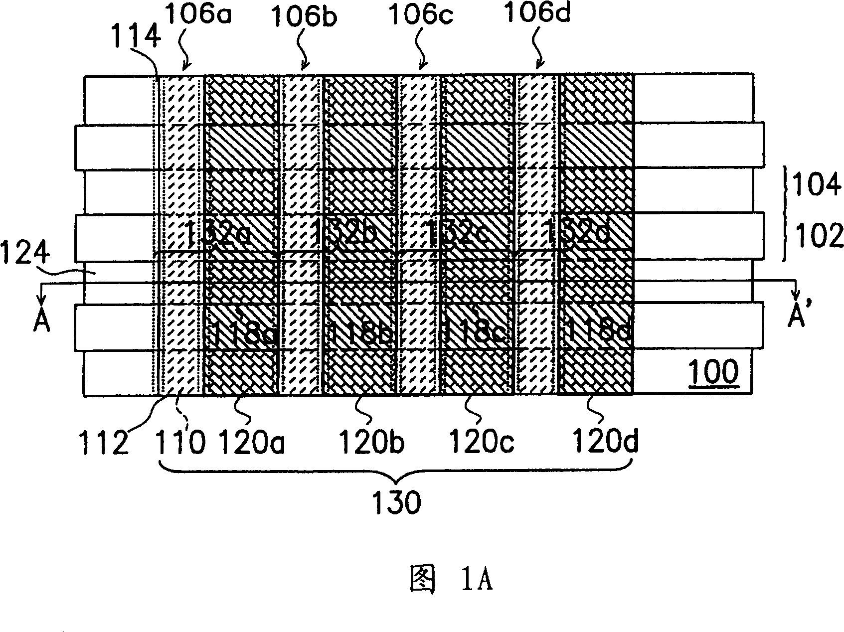
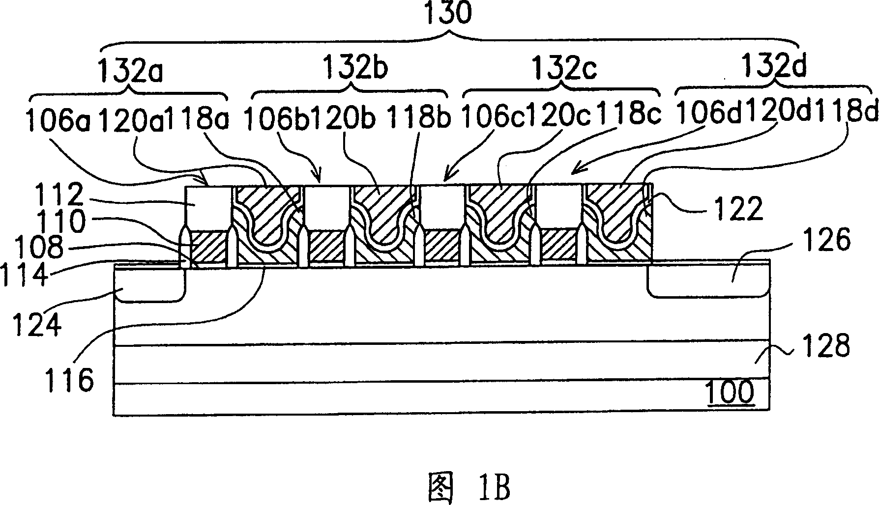
[0045] FIG. 1A is a top view showing a NAND type flash memory cell array of the present invention. Fig. 1B is a cross-sectional view showing the structure along line A-A' in Fig. 1A.

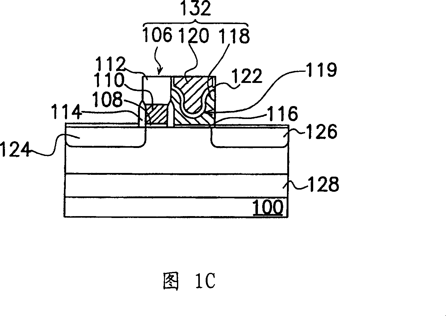
[0046] Please refer to FIG. 1A and FIG. 1B at the same time. The flash memory cell array structure of the present invention is at least composed of a substrate 100, an element isolation structure 102, an active region 104, and a plurality of stacked gate structures 106a-106d (each stacked gate structure 106a-106d are sequentially from the substrate 100 the selection gate dielectric layer 108, the selection gate 110, the top cover layer 112), the spacer 114, the tunneling dielectric layer 116, and a plurality of floating gates 118a-118d , a plurality of control gates 120 a - 120 d , an inter-gate dielectric layer 122 , a drain region 124 , and a source region 126 .

[0047] The substrate 100 is, for example, a P-type silicon substrate, and a deep N-type well region 128 is provided in the substra...


PUM


Abstract

The present invention discloses a flash memory storage unit, flash memory storage unit array and its making method. Said flash memory storage unit array consists of substrate, series-connected several storage unit structures and source region / drain region. Every storage unit structure is formed from stack gate structure consisting of selection gate dielectric layer, selection gate and top cover layer; gap wall placed on the side wall of selection gate; control gate which is placed on one side of the stack gate structure and is connected with stack gate structure; floating gate placed between control gate and substrate; intergate dielectric layer placed between the control gate and floating gate; tunneling dielectric layer placed between floating gate and substrate and control gate and source region / drain region respectively placed in the most external side of storage unit array and substrate of one side of stack gate structure.

Description

technical field [0001] The present invention relates to a semiconductor device, and in particular to a flash memory unit and a manufacturing method thereof. Background technique [0002] Flash memory elements have the advantages of being able to store, read, and erase data multiple times, and the stored data will not disappear after power failure, so it has become a widely used device in personal computers and electronic devices. A non-volatile memory element. [0003] A typical flash memory device uses doped polysilicon to make a floating gate (Floating Gate) and a control gate (Control Gate). Moreover, the floating gate is separated from the control gate by a dielectric layer, and the floating gate is separated from the substrate by a tunnel oxide layer (Tunnel Oxide). When performing write / erase (Write / Erase) data operations on the flash memory, by applying a bias voltage to the control gate and source / drain regions, electrons are injected into the floating gate or elec...

Claims


Application Information

Patent Timeline
Patent Type & Authority Patents(China)
IPC IPC(8): H01L27/105H01L27/115H01L21/8239H01L21/8247
Inventor 许正源洪至伟吴齐山黄明山
Owner POWERCHIP SEMICON CORP
Why Eureka
Try Eureka