Fingerprint chip electrical performance testing device

An electrical performance testing and fingerprint chip technology, applied in the field of fingerprint identification, can solve the problems such as the inability of automatic feeding, indexing and conveying of fingerprint chips, low testing efficiency, etc., and achieve the effects of simple and practical structure, simple and practical structure, and good separation effect.

Active Publication Date: 2018-05-18
HANGZHOU CHANGCHUAN TECH CO LTD
View PDF8 Cites 9 Cited by
  • Summary
  • Abstract
  • Description
  • Claims
  • Application Information

AI Technical Summary

Problems solved by technology

[0003] The purpose of the present invention is to overcome the shortcomings of the current fingerprint identification chip detection device that the fingerprint chip cannot be automatically loaded, transposed and transported, and the test efficiency is low, and to provide a fingerprint chip that can be automatically loaded, transpositioned and transported, and the test efficiency is relatively high. High fingerprint chip electrical performance testing device

Method used


Image

  • Fingerprint chip electrical performance testing device
  • Fingerprint chip electrical performance testing device
  • Fingerprint chip electrical performance testing device

Examples


Embodiment Construction

[0040] The present invention will be further described below in conjunction with the accompanying drawings.

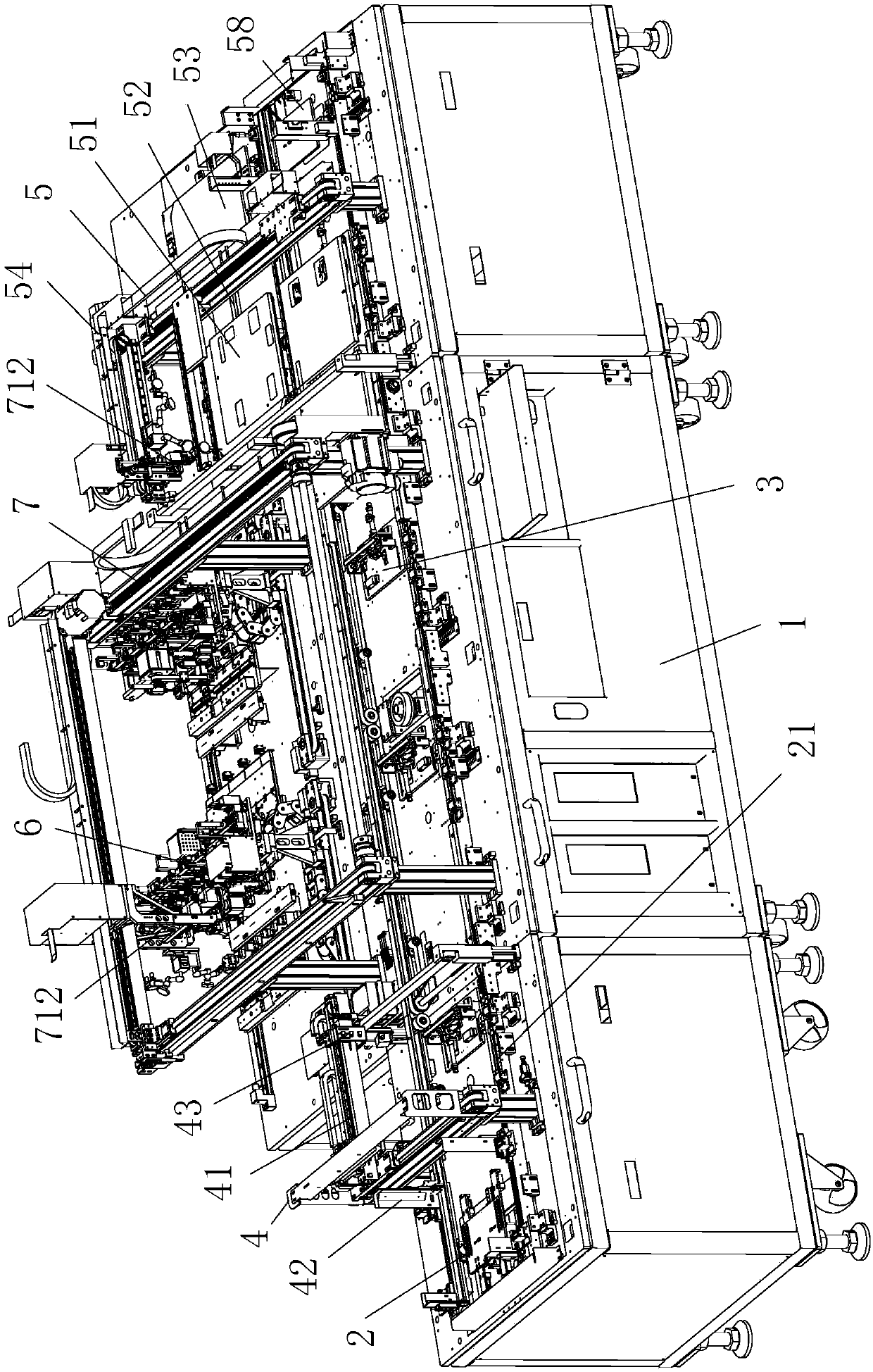
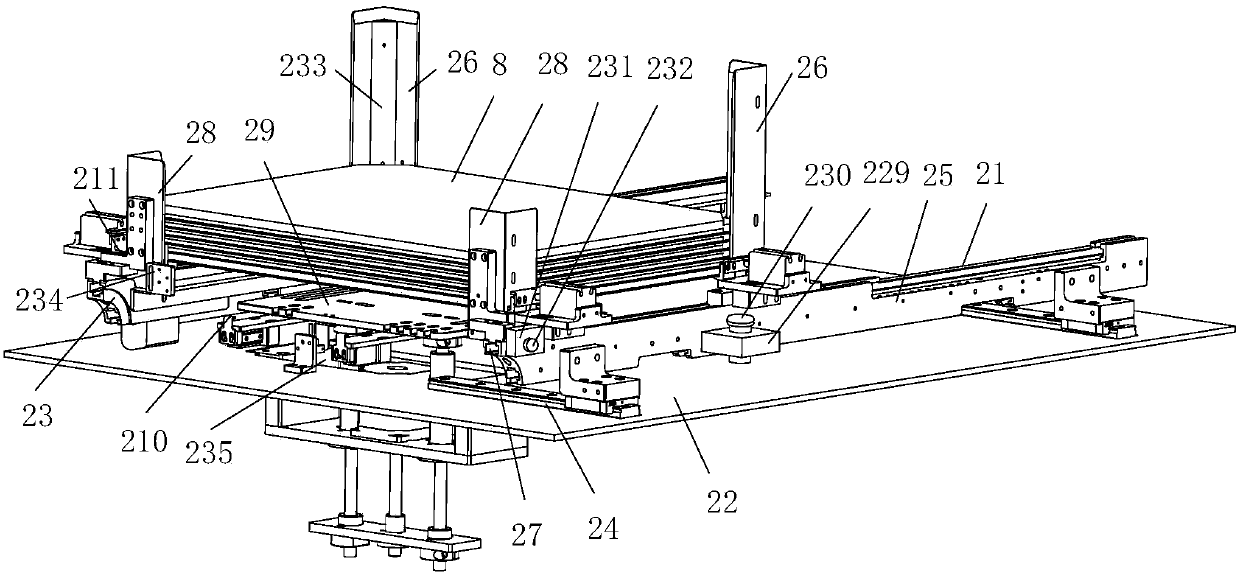
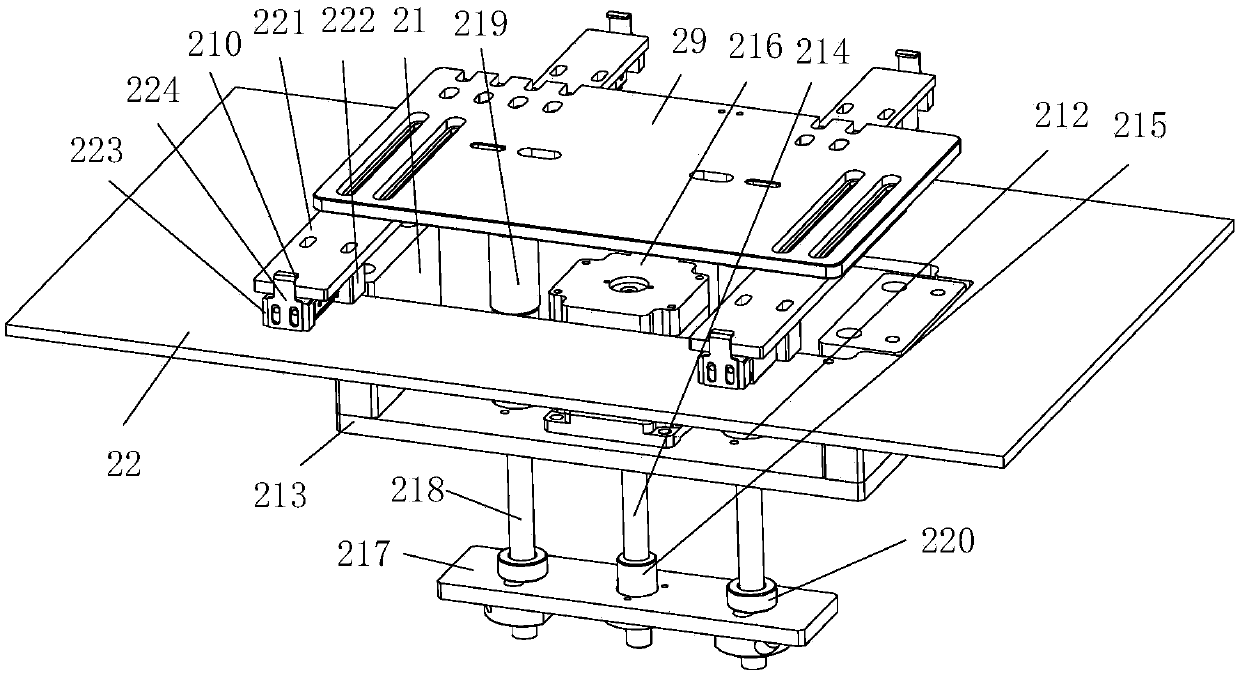
[0041] as attached figure 1 to attach Figure 16 Shown: a device for testing electrical properties of fingerprint chips, including: a testing system, a feeding system, and a receiving system; The tray positioning device 3 arranged front and back between the two tray conveyor belts 21 is provided with a fingerprint chip identification number recognition device 4 of a machine vision system 41 located above the first tray positioning device 3, and a fingerprint chip identification number recognition device 4 located at the last tray positioning device 3 is provided. The receiving system 5 of the adsorption mechanism above the tray positioning device 3; the test system includes: two test devices 6 that are symmetrically arranged and located on the outside of the side of the sub-disc conveying device 2, and are provided with the test device 6 and the rest of the tray positio...


PUM


Abstract

The present invention relates to a fingerprint chip electrical performance testing device. The fingerprint chip electrical performance testing device includes a testing system, a feeding system, and amaterial collection system; the feeding system includes a tray separating and conveying device, a plurality of tray positioning devices, a fingerprint chip number identification device, and a material collection system, wherein the tray separating and conveying device is provided with two tray delivering conveyor belts, the plurality of tray positioning devices are arranged between the two tray delivering conveyor belts, the fingerprint chip number identification device is provided with a machine vision system located above the first tray positioning device, the material collection system isprovided with an adsorption mechanism located above the last tray positioning device; and the test system includes two test devices and material taking devices, wherein the two test devices are arranged symmetrically outside one side of the tray separating and conveying device, and the material taking devices are located at the test devices and adsorption devices located above the other tray positioning devices. The fingerprint chip electrical performance testing device can automatically feed, transfer and convey fingerprint chips and has high test efficiency.

Description

technical field [0001] The invention relates to the field of fingerprint identification, in particular to a device for testing electrical performance of a fingerprint chip. Background technique [0002] Communication equipment is updated with each passing day, and information security is becoming more and more important. With the development of communication equipment, fingerprint recognition technology has become more and more mature and has been widely used; To ensure the quality of the fingerprint chip; the structure of the fingerprint chip testing machine can be understood from a fingerprint recognition chip detection device disclosed in the invention of the application number: 201410803544.1; the traditional fingerprint recognition chip detection device has the problem that the fingerprint chip cannot be automatically loaded and transposed Therefore, it is an urgent problem to design a fingerprint chip electrical performance testing device that can automatically load an...

Claims


Application Information

Patent Timeline
Patent Type & Authority Applications(China)
IPC IPC(8): G01R31/28
CPCG01R31/2856
Inventor 韩笑陈思乡姜传力翁水才鲍军其谢周阳刘治震章华荣
Owner HANGZHOU CHANGCHUAN TECH CO LTD
Why Eureka
Try Eureka