A Photodetector Location Layout for Large Displacement Monitoring

A photodetector and large displacement technology, applied in the field of photodetectors, can solve the problems of inability to simultaneously apply distance position monitoring, parasitic capacitance reduces bandwidth, troublesome output processing, etc., and achieves simple result processing, saving area, and small output quantity Effect

Active Publication Date: 2020-12-01
XIAMEN UNIV
View PDF5 Cites 0 Cited by
  • Summary
  • Abstract
  • Description
  • Claims
  • Application Information

AI Technical Summary

Problems solved by technology

Although this method has low power consumption, it results in low resolution and cannot be applied to distance position monitoring at the same time.
[0006] However, miniaturization is the main direction of MOEMS. Excessive PD arrangement greatly increases the area of ​​the chip and the volume of the system; and multiple PDs have more power consumption, and their output processing is more troublesome; a single PD If the area is too large, although the responsivity will be improved, the parasitic capacitance will greatly reduce the bandwidth

Method used


Image

  • A Photodetector Location Layout for Large Displacement Monitoring
  • A Photodetector Location Layout for Large Displacement Monitoring
  • A Photodetector Location Layout for Large Displacement Monitoring

Examples


Embodiment Construction

[0016] The following embodiments will further illustrate the present invention in conjunction with the accompanying drawings, and the monitored entity will take a common micromirror as an example.

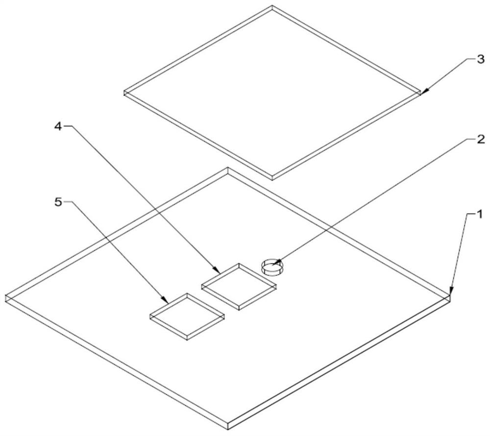
[0017] see figure 1 , Schematic diagram of the photodetector layout of the present invention. 1 is chip substrate, 2 is light source, 3 is micromirror, 4 is PD A , 5 for PD B . In practice, the light source is driven by an emission drive circuit inside the chip to emit light, and the upper micromirror is displaced vertically. The reflected light is received by the PD for photoelectric conversion, and other circuits on the chip amplify and convert the current signal of the two PDs. , for analysis.

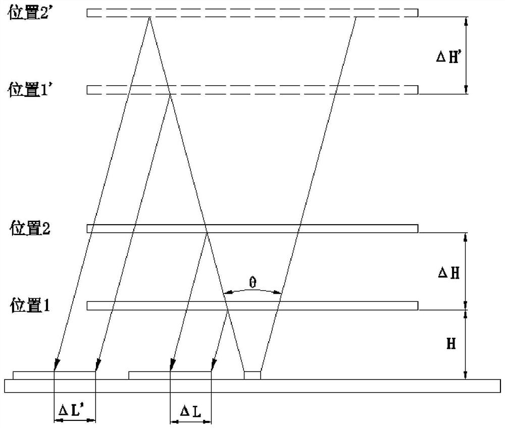
[0018] see figure 2 , Schematic diagram of reflected light in the present invention. ΔH and ΔH' are the height changes of the corresponding micromirrors within the receiving range of the two PDs, respectively. The optical power of the light source is P, the emission angle of the ...


PUM


Abstract

The invention, which relates to the photoelectric detector field, provides photoelectric detector location layout for large displacement monitoring. The layout is as follows: two square PDs are arranged at the same side of a light source; one side of each PD is adjacent to the light source; and reflected light of the light source irradiates the PDs. Large displacement monitoring of the object location is realized by using only two PDs; the outputted linear zone is extended; segmented processing is realized; and the great convenience is provided for monitoring different displacement ranges. Thehigh resolution and high sensitivity are realized; the layout is easy to control; the result processing becomes simple and conveniently; the cost is low; and current sheet processing becomes convenient. When the light intensity corresponding to the PD at the outer side is processed, the light intensity of the processed PD is compared with the light intensity of the PD at the inner side, so that the illumination influence on the result is reduced to the great extent. Diversified monitoring functions are realized only based on the analog circuit design; the output number is reduced; the need ofa large-scale digital signal for processing the array type output is avoided; and the chip area is saved.

Description

technical field [0001] The invention relates to a photodetector, in particular to a position layout of a photodetector for large-displacement monitoring in which two photodetectors are placed on the same side of a light source to realize a monitoring function. Background technique [0002] Optical position sensors use optical signals to complete the measurement of monitoring entities. The light signal emitted by the light source is reflected by the object and becomes the incident light signal which is captured by the detector. According to the change of the position of the monitoring entity, the optical signal received by the detector will also change, so as to monitor the change of the output signal, such as the displacement of the scanning micromirror (Yang Tingyan, Wen Zhiyu, Zhou Ying. High-efficiency scanning for miniature near-infrared spectrometers Grating Micromirror Design. Detection of Intense Laser and Particle Beam, 2016, 28(6): 1-6). As the core component of m...

Claims


Application Information

Patent Timeline
Patent Type & Authority Patents(China)
IPC IPC(8): G01B11/02
CPCG01B11/02
Inventor 程翔刘岩孙兴林
Owner XIAMEN UNIV
Why Eureka
Try Eureka