Vertical structure LED chip based on GaN material and preparation method thereof
An LED chip, vertical structure technology, applied in electrical components, circuits, semiconductor devices, etc., can solve the problems of difficult packaging, poor reliability, etc., to achieve the effect of flexible color temperature, reduce consumption, and improve integration.
- Summary
- Abstract
- Description
- Claims
- Application Information
AI Technical Summary
Problems solved by technology
Method used
Image

Examples
Embodiment 1
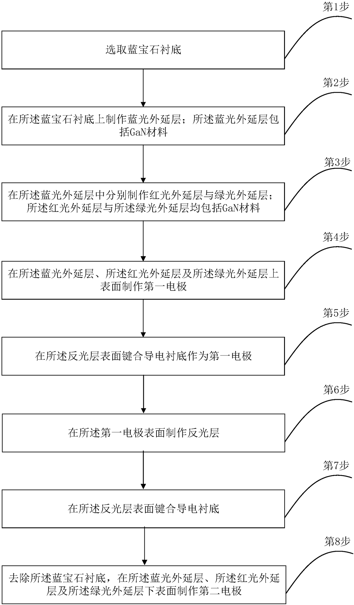
[0054] See figure 1 , figure 1 A flow chart of a method for preparing a GaN material-based vertical structure LED chip provided by an embodiment of the present invention, the preparation method includes:
[0055] (a) select a sapphire substrate;
[0056] (b) making a blue epitaxial layer on the sapphire substrate;
[0057] (c) making a red epitaxial layer and a green epitaxial layer respectively in the blue epitaxial layer;
[0058] (d) making a first electrode on the upper surface of the blue epitaxial layer, the red epitaxial layer and the green epitaxial layer;
[0059] (e) making a reflective layer on the surface of the first electrode;
[0060] (f) bonding a conductive substrate on the surface of the reflective layer;
[0061] (g) removing the sapphire substrate, and fabricating a second electrode on the lower surfaces of the blue epitaxial layer, the red epitaxial layer, and the green epitaxial layer.
[0062] Wherein, the crystal plane of the sapphire substrate is...
Embodiment 2
[0103] This embodiment uses an example on the basis of Embodiment 1 to illustrate the implementation of this solution.
[0104] Please refer to Figure 3a ~ Figure 3i , Figure 3a ~ Figure 3i It is a schematic diagram of a method for preparing a GaN material-based vertical structure LED chip according to an embodiment of the present invention. Specifically, the preparation method comprises the following steps:
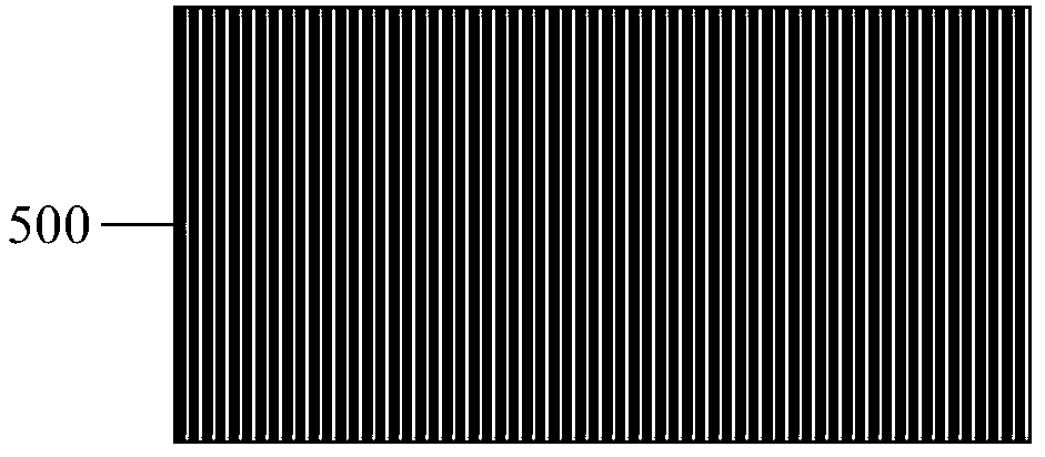
[0105] Step 1, select a sapphire substrate 500 with a thickness of 4000nm, such as Figure 3a shown.
[0106] Step 2. At a temperature of 500° C., grow an N-type GaN material with a thickness of 4000 nm on the upper surface of the sapphire substrate 500 as the first buffer layer 501; An N-type GaN material with a thickness of 1000 nm is grown on the surface as the first stable layer 502; at a temperature of 1000° C., a thickness of 400 nm is grown on the surface of the first stable layer 502, and the doping concentration is 1×10 19 cm -3 The N-type GaN material i...
Embodiment 3
[0115] This embodiment is based on the preparation method described in the above embodiments, focusing on the description of the structure of the LED chip.
[0116] Specifically, please refer to Figure 4 , Figure 4 It is a schematic structural diagram of a GaN material-based vertical structure LED chip according to an embodiment of the present invention. The LED chip 400 includes: a conductive substrate 401, a reflective layer 402, a first electrode 403, a blue epitaxial layer 404, a red epitaxial layer 405, a green epitaxial layer 406, a second electrode 407, a passivation layer 408 and an isolation layer 409 .
[0117] Wherein, the conductive substrate 401 can adopt materials with good conductivity such as copper plate, aluminum plate or heavily doped silicon wafer; the reflective layer 402 adopts metal materials with good reflective properties, such as Ni, Pb, Ni / Pb alloy or Al; The electrode 403 and the second electrode 407 are preferably Ni, copper and other material...
PUM
| Property | Measurement | Unit |
|---|---|---|
| Thickness | aaaaa | aaaaa |
| Thickness | aaaaa | aaaaa |
| Thickness | aaaaa | aaaaa |
Abstract
Description
Claims
Application Information
 - R&D
- Intellectual Property
- Life Sciences
- Materials
- Tech Scout
- Unparalleled Data Quality
- Higher Quality Content
- 60% Fewer Hallucinations
Browse by: Latest US Patents, China's latest patents, Technical Efficacy Thesaurus, Application Domain, Technology Topic, Popular Technical Reports.
© 2025 PatSnap. All rights reserved.Legal|Privacy policy|Modern Slavery Act Transparency Statement|Sitemap|About US| Contact US: help@patsnap.com